background image

TH-103PF10WK/TK/RK

19

6.1.2.

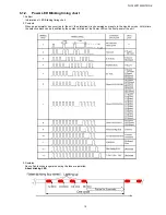
Power LED Blinking timing chart

1. Subject

Information of LED Blinking timing chart.

2. Contents

When an abnormality has occurred to  the unit, the protection circuit operates and resets to the stand by mode. At this time,
the defective block can be identified by the number of blinks of the Power LED on the front panel of the unit.

3. Remarks

Above Fan function is operated during the fans are installed.

About blinking LED

Summary of Contents for TH-103PF10WK

Page 1: ...Power 20 6 3 No Picture 20 6 4 Local screen failure 21 7 Disassembly and Assembly Instructions 22 7 1 Rear Cover and Board 22 7 2 Location of Rear Cover screws 23 7 3 Removal of Side Angle L R 26 7 4 Removal of HA Board 27 7 5 Removal of HDMI Board 28 7 6 Removal of DS Board 28 7 7 Removal of HX Board 28 7 8 Removal of DN Board 29 7 9 Removal of PB Board 29 7 10 Removal of H5 Board 29 7 11 Removal...

Page 2: ...k Diagram 75 9 10 DS Board 2 of 2 Block Diagram 76 9 11 DN Board 1 of 2 Block Diagram 77 9 12 DN Board 2 of 2 Block Diagram 78 9 13 D Board 1 of 2 Block Diagram 79 9 14 D Board 2 of 2 Block Diagram 80 9 15 C1 C2 CY and CZ Board Block Diagram 81 9 16 C2 C3 CX and CY Board Block Diagram 82 9 17 C4 C5 C8 and C9 Board Block Diagram 83 9 18 C5 C6 C7 and C8 Board Block Diagram 84 9 19 SC2 and S1 Board B...

Page 3: ...tween the jumpered AC plug and each exposed metal lic cabinet part on the equipment such as screwheads connectors control shafts etc When the exposed metal lic part has a return path to the chassis the reading should be between 1Mohm and 5 2Mohm When the exposed metal does not have a return path to the chassis the reading must be Figure 1 1 1 2 Leakage Current Hot Check See Figure 1 1 Plug the AC ...

Page 4: ...r exposure of the assembly 3 Use only a grounded tip soldering iron to solder or unsolder ES devices 4 Use only an anti static solder removal device Some solder removal devices not classified as anti static ESD protected can generate electrical charge sufficient to damage ES devices 5 Do not use freon propelled chemicals These can generate electrical charges sufficient to damage ES devices 6 Do no...

Page 5: ...ion Pb free solder has a higher melting point than standard solder Typically the melting point is 50 70 F 30 40 C higher Please use a high temperature soldering iron and set it to 700 20 F 370 10 C Pb free solder will tend to splash when heated too high about 1100 F or 600 C If you must use Pb solder please completely remove all of the Pb free solder on the pins or solder area before applying Pb s...

Page 6: ...TH 103PF10WK TK RK 6 3 Service Navigation 3 1 Service Hint ...

Page 7: ...wer Switch SS2 Sustain Out Upper SS3 Sustain Out Lower V1 LED_G R SS Sustain Drive V2 Key Scan SC Scan Drive V3 Remocon Receiver SC2 DC DC Converter For Scan Drive PB Fan Control SU Scan Out Upper P SUS_1 2 Power Supply SM Scan Out Middle P MULTI_1 2 Power Supply SD Scan Out Lower F Line Filter C1 Data Drive 1 PC Power Control C2 Data Drive 2 HX PC RS 232C C3 Data Drive 3 HA BNC Component Video C4...

Page 8: ...TH 103PF10WK TK RK 8 3 2 Applicable signals ...

Page 9: ...TH 103PF10WK TK RK 9 ...

Page 10: ...HDMI A B TYPE A Connector x 2 COMPONENT RGB IN Y G BNC with sync 1 0 Vp p 75 ohm PB B BNC PR R BNC 0 7 Vp p 75 ohm AUDIO IN RCA PIN JACK 2 0 5 Vrms high impedance PC IN HIGH DENSITY Mini D SUB 15PIN Y or G with sync 1 0 Vp p 75 ohm Y or G without sync 0 7 Vp p 75 ohm B PB CB 0 7 Vp p 75 ohm R PR CR 0 7 Vp p 75 ohm HD VD 1 0 5 0 Vp p high impedance AUDIO IN M3 JACK 0 5 Vrms high impedance SERIAL EX...

Page 11: ...ode and switch off the main power 5 1 1 IIC mode Select the IIC mode by Up Down button on the remote control at the front page of CAT mode and then press the Action button on the remote control Subject and item are mentioned on IIC mode structure To exit the IIC mode press the R button on the remote control ...

Page 12: ...n IC4002 this version can be upgrade by 1 replace of new version IC 2 Loading the new version software from loader tool TZSC07036 Memory data change To exit the CD mode press the R button on the remote control 5 1 3 SD mode Select the SD mode by Up Down button on the remote control at the front page of CAT mode and then press the Action button on the remote control To exit the SD mode press the R ...

Page 13: ...ld be set after exchange of DN Board Destination number Default setting Number Destination Number Destination 0 Japan 16 1 North America 17 2 Europe 18 China 3 Others 19 China Hotel 4 Britain 20 Russia 5 Taiwan 21 Russia Hotel 6 Thailand 22 Hong Kong 7 23 8 Japan Hotel 24 9 North America Hotel 25 10 Europe Hotel 26 11 27 12 Britain Hotel 28 Middle East Hong Kong 13 29 Middle East Hong Kong Hotel 1...

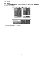
Page 14: ...ID mode Select the ID mode by Up Down button on the remote control at the front page of CAT mode and then press the Mute button on the remote control more than 3 seconds To exit the ID mode press the R button on the remote control ...

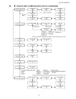
Page 15: ...TH 103PF10WK TK RK 15 5 2 IIC mode structure following items value is sample data ...

Page 16: ...TH 103PF10WK TK RK 16 5 3 Option Setting ...

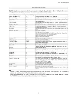
Page 17: ...alidation Off Valid key is all key of remote User1 Valid key are only Stand by ON OFF Input Direct input Status Sur round Sound mute On Off and volume adjustment User2 Valid key is only Stand by ON OFF User3 All keys are null and void Advanced PIP Off Off Sets normal two screen display mode On Sets Advanced PIP mode Off timer function Enable Off timer operation Enable Disable Initial Power Mode No...

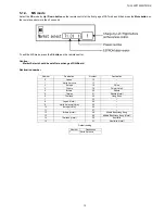
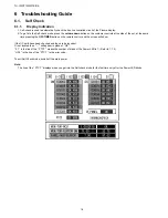
Page 18: ...ame time pressing the OFF TIMER button on the remote control and the screen will show If the IIC ports have been checked and found to be incorrect Or not located then will appear in place of OK 01 in the line of the PTCT means the number of blinks of the Power LED is 1 Refer to 7 1 2 H09 in the line of the PTCT is the error code To exit Self Check mode switch off the main power Note The line of th...

Page 19: ... When an abnormality has occurred to the unit the protection circuit operates and resets to the stand by mode At this time the defective block can be identified by the number of blinks of the Power LED on the front panel of the unit 3 Remarks Above Fan function is operated during the fans are installed About blinking LED ...

Page 20: ...10WK TK RK 20 6 2 No Power First check point There are following 3 states of No Power indication by power LED 1 No lit 2 Green is lit then turns red blinking a few seconds later 3 Only red is lit 6 3 No Picture ...

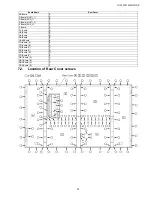
Page 21: ...TH 103PF10WK TK RK 21 6 4 Local screen failure Plasma display may have local area failure on the screen Fig 1 is the possible defect P C B for each local area Fig 1 ...

Page 22: ...oard Rear Cover required to remove for each board exchange Board Name Rear Cover D Board D DS Board B SS Board F SC Board A B C SC2 Board A C SU Board A SM Board A SD Board A C1 Board A C2 Board A B C3 Board B D C4 Board B D C5 Board D F C6 Board F C7 Board F C8 Board E F C9 Board C E CX Board C E CY Board A C CZ Board A H5 Board B S1 Board A SS2 Board F SS3 Board F V1 Board A B C D E F V2 Board A...

Page 23: ...TI_1 E P Board SUS_1 E P Board MULTI_2 C P Board SUS_2 C F Board E PC Board D HX Board B HA Board B DN Board B HDMI Board B CD Board A B CD Board B D CD Board C D CD Board D D CD Board E D CD Board F B DR1 Board A A DR1 Board B F DR2 Board A A DR2 Board B F Board Name Rear Cover ...

Page 24: ...ear Cover A 1 Remove Eye Bolt Covers 2 Remove screws 21 2 and then remove the Rear Cover A 7 2 2 Removal of Rear Cover B 1 Remove screws 21 7 and then remove the Rear Cover B Tighten screw first in order of and when mount ing the Rear cover B ...

Page 25: ...Rear Cover C 7 2 4 Removal of Rear Cover D 1 Remove screws 21 and then remove the Rear Cover D Tighten screw first in order of and when mounting the Rear cover D 7 2 5 Removal of Rear Cover E 1 Remove screws 25 and then remove the Rear Cover E Tighten screw first in order of and when mounting the Rear cover E 7 2 6 Removal of Rear Cover F 1 Remove Eye Bolt Covers ...

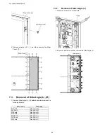
Page 26: ...orehand when remove the following Boards 7 3 1 Removal of Side Angle L 1 Remove 4 screws A of the Plate 2 Remove 19 screws and then remove the Side Angle L Board name Side Angle SU Board Side Angle R SM Board Side Angle R SD Board Side Angle R SC Board Side Angle R SS2 Board Side Angle L SS3 Board Side Angle L SS Board Side Angle L ...

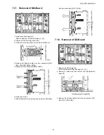
Page 27: ...he Side Power Unit upward 3 Remode the side Power Unit 4 Remove 4 screws B of the Plate 5 Remove 19 screws and then remove the Side Angle R 7 4 Removal of HA Board 1 Remove 4 screws C and then remove the HA Terminal Block 2 Remove 4 screws D and remove Shield Plate 3 Remove 2 Hexagonal Head screws E and then remove HA Board ...

Page 28: ...nnect the connectors DS1 DS2 DS3 DS4 DS6 DS9 DS10 DS14 DS15 DS30 2 Remove 5 screws and then remove the Slot Block Case 3 Remove 11 screws and then remove DS Board 7 7 Removal of HX Board 1 Remove the HA Terminal Block Refer to Removal of HA Board 2 Remove the HDMI Terminal Block Refer to Removal of HDMI Board 3 Disconnect the connectors HX1 4 Remove 4 screws and then remove the Slot Block Case 5 R...

Page 29: ...isconnect the connectors DN2 DN3 DN5 3 Remove 4 screws and then remove DN Board 7 9 Removal of PB Board 1 Disconnect the connectors PB30 PB31 PB51 PB53 PB54 PB56 PB59 PB61 PB62 PB64 PB66 PB69 PB71 2 Remove 4 screws and then remove PB Board 7 10 Removal of H5 Board 1 Disconnect a connector H51 2 Remove 2 screws and then remove H5 Board Block ...

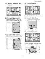
Page 30: ...Remove 4 screws and then remove D Board 7 12 Removal of P Board MULTI_1 MULTI_2 The fuses are not included in P Board for the repair 7 12 1 Removal of P Board MULTI_1 1 Disconnect the connectors P5 P12 P25 P51 P53 P55 2 Remove 9 screws and then remove P Board MULTI_1 7 12 2 Removal of P Board MULTI_2 1 Disconnect the connectors P5 P10 P12 P23 P25 P51 P53 P55 2 Remove 9 screw and then remove P Boar...

Page 31: ...S_1 7 13 2 Removal of P Board SUS2 1 Disconnect the connectors P2 P9 P11 P52 P54 P56 2 Remove 10 screws and then remove P Board SUS_2 7 14 Removal of F Board The fuses F900 F901 F903 F904 are not included in F Board for the repair 1 Disconnect the connectors F1 F8 F9 2 Remove 5 screws and then remove F Board 7 15 Removal of PC Board 1 Disconnect the connectors PC201 PC202 PC203 PC204 PC205 2 Remov...

Page 32: ...n relay connectors 4 Remove 4 screws and then remove the Fan Block A B 5 Remove the flexible cables from the connectors SU1 SU2 SU3 SU4 SU55 6 Disconnect the connector SU45 7 Remove 9 screws 8 Slide the SU Board to the upper direction to remove the SU Board from the connectors SU41 SU42 Take out so as not to damage SU Board 9 Slide the SU Board to the bottom direction to remove the SU Board ...

Page 33: ...ble cables from the connectors SM1 SM2 SM3 SM4 SM55 SM56 5 Disconnect the connectors SM50 SM51 6 Remove 8 screws 7 Slide SM Board to the left direction to remove SM Board from the connectors SC43 SC46 7 18 Removal of SD Board 1 Remove the Side Angle R Refer to Removal of the Side Angle L R 2 Remove 6 screws and then remove the Reinforcement Angle B 3 Remove the flexible cables from the connectors ...

Page 34: ...SD Board 7 Slide the SD Board to the upper direction to remove the SD Board 7 19 Removal of SC Board 1 Remove SU Board Refer to Removal of SU Board 2 Remove SM Board Refer to Removal of SM Board 3 Remove SD Board Refer to Removal of SD Board 4 Remove the Eye Bolt and Eye Bolt Cover 5 Remove 5 screws and then remove the Rear Cover Angle A 6 Disconnect the connectors SC2 SC20 SC23 SC80 SC81 ...

Page 35: ...tors SC12 SC13 SC14 SC34 SC82 SC83 SC84 2 Remove 4 screws and then remove SC2 Board 7 21 Removal of S1 Board and V2 Board 7 21 1 Removal of S1 Board 1 Remove the Side Power Unit Reference to Removal of the Side Angle L R 2 Remove 2 screws K 3 Remove 1 screw L 4 Disconnect the connector S34 and then remove S1 Board s ...

Page 36: ... Angle L R 2 Disconnect the Fan relay connectors 3 Remove 6 screws and then remove the Fan D and Fan Block E 4 Remove 6 screws and then remove the Reinforcement Angle E 5 Remove the flexible cables from the connectors SS29 SS30 SS51 SS52 SS53 SS54 6 Remove 6 screws and then remove SS2 Board 7 23 Removal of SS3 Board 1 Remove the Side Angle L Refer to Removal of Side Angle L R 2 Disconnect the Fan ...

Page 37: ...from the connectors SS36 SS37 SS59 SS60 SS61 SS62 9 Remove 6 screws and then remove SS3 Board 7 24 Removal of SS Board 1 Remove the Side Angle L Refer to Removal of Side Angle L R 2 Disconnect the Fan relay connectors 3 Remove 4 screws and then remove the Fan Block F G 4 Remove the flexible cables from the connectors SS21 SS23 SS26 SS27 SS55 SS56 SS57 SS58 5 Disconnect the connectors SS2 SS13 SS35...

Page 38: ...n relay connectors 2 Remove each 4 screws of Fan Block A B E H J and then remove the Fan Blocks 3 Remove each 4 screws of Fan C F G and then remove the Fans 4 Remove each 3 screws of Fan D K and then remove the Fans 5 Remove each 4 screws and then remove the Fans ...

Page 39: ...hen remove the Reinforce ment Angle A 3 Remove 4 screws of the flexible cable 4 Disconnect the connector C14 5 Remove the flexible cables from the connectors CA1 CA2 C11 6 Remove 4 screws and then remove C1 Board 7 27 Removal of C2 Board 1 Remove the Fan Block A B Refer to Removal of Fan 2 Remove the Eye Bolt and Eye Bolt Cover 3 Remove 5 screws and then remove the Rear Cover Angle A ...

Page 40: ... the connectors C22 C24 8 Remove 6 screws and then remove C2 Board 7 28 Removal of C3 Board 1 Remove the Eye Bolt 2 Remove 5 screws and then remove the Rear Cover Angle C 3 Remove 6 screws and then remove the Reinforcement Angle C 4 Remove 6 screws of the flexible cable 5 Remove the flexible cables from the connectors CA6 CA7 CA8 C31 C32 6 Disconnect the connector C34 7 Remove 5 screws and then re...

Page 41: ...4 6 Remove 5 screws and then remove C4 Board 7 30 Removal of C5 Board 1 Remove the Eye Bolt and Eye Bolt Cover 2 Remove 15 screws and then remove the Fan C D and Fan Block E F 3 Remove 5 screws and then remove the Rear Cover Angle E 4 Remove 2 screws of Side Angle L 5 Remove 6 screws and then remove the Reinforce ment Angle E 6 Remove 6 screws of the flexible cable 7 Remove the flexible cables fro...

Page 42: ...from the connectors CA15 CA16 C61 5 Disconnect the connector C64 6 Remove 4 screws and then remove C6 Board 7 32 Removal of C7 Board 1 Remove 7 screws and then remove the Fan Block G and Fan K 2 Remove 2 screws and then remove the Rear Cover Angle H 3 Remove the Eye Bolt Covers 4 Remove 5 screws and then remove the Rear Cover Angle F 5 Remove 2 screws of Side Angle L 6 Remove 6 screws and then rem...

Page 43: ...ear Cover Angle F H Refer to Removal of C7 Board 3 Remove the Reinforcement Angle F Refer to Removal of C7 Board 4 Remove 6 screws of the flexible cable 5 Remove the flexible cables from the connectors CB12 CB13 CB14 C80 C81 C83 6 Disconnect the connectors C82 C84 C88 7 Remove 6 screws and then remove C8 Board 7 34 Removal of C9 Board 1 Remove 4 screws and then the Rear Cover Angle G H 2 Remove 5 ...

Page 44: ... G H Refer to Removal of C9 Board 2 Remove the Reinforcement Angle D Refer to Removal of C9 Board 3 Remove 6 screws of the flexible cable 4 Remove the flexible cables from the connectors CB6 CB7 CB8 CX1 CX2 5 Disconnect the connector CX4 6 Remove 5 screws and then remove CX Board 7 36 Removal of CY Board 1 Remove 2 screws and then the Rear Cover Angle G 2 Remove 2 Eye Bolt Covers 3 Remove 5 screws...

Page 45: ...7 37 Removal of CZ Board 1 Remove the Reinforcement Angle B Refer to Removal of CY Board 2 Remove 4 screws of the flexible cable 3 Disconnect the connector CZ4 4 Remove the flexible cables from the connectors CB1 CB2 CZ1 5 Remove 4 screws and then remove CZ Board 7 38 Removal of DR1 Board A 1 Disconnect the Fan relay connectors 2 Remove 4 screws and then remove the Fan Block B 3 Disconnect the con...

Page 46: ...to the connector DR6 7 40 Removal of DR2 Board A 1 Disconnect the connectors DR11 DR12 DR13 DR14 DR15 2 Remove 5 screws and then remove DR2 Board A 7 41 Removal of DR2 Board B Attaching short jumper to connector DR16 Attach Short Jumper to the connector DR16 when replacing DR2 Board 1 Remove 4 screws and then remove Fan Block E 2 Disconnect the connectors DR11 DR12 DR13 DR14 DR15 3 Remove 5 screws...

Page 47: ...s CD1 CD2 2 Remove 2 screws and then remove CD Board B 7 42 3 Removal of CD Board C 1 Remove the flexible cables from the connectors CD1 CD2 2 Remove 2 screws and then remove CD Board C 7 42 4 Removal of CD Board D 1 Remove the Fan Block H Refer to Removal of the Fan 2 Remove the flexible cables from the connectors CD1 CD2 3 Remove 2 screws and then remove CD Board D 7 42 5 Removal of CD Board E 1...

Page 48: ...CD2 3 Remove 2 screws and then remove CD Board F 7 43 Removal of AC Inlet 1 Remove 2 screws and then remove the AC Inlet Cover 2 Disconnect a connector F1 3 Remove 3 screws and then remove the AC Inlet 7 44 Removal of Cabinet and Front Glass 7 44 1 Removal of Front Glass 1 Disconnect the connectors DS15 SC34 2 Remove 4 screws and then side the Side Power Unit upward 3 Remode the side Power Unit 4 ...

Page 49: ...and bottom side and then remove the Fixed Angles A B C D 6 Remove the Front Glass Note When removing the Front Glass from Cabinet there is a risk of the glass center bending damage Be sure to lift the instruction six positions of the figure when remove the Front Glass Note When replacing the Front Glass The sponges for the Front Glass cannot be recycled When replacing the Front Glass use the new s...

Page 50: ...d then remove the Con nection Angles A AS B BS 3 Remove the Cabinet Top 7 44 2 2 Removeval of Cabinet Bottom 1 Remove each 5 screws 2 Remove each 2 screws and then remove the Con nection Angles A AS B BS 3 Remove the Cabinet Bottom 7 44 2 3 Removeval of Cabinet Right 1 Remove each 5 screws 2 Remove each 2 screws and then remove the Con nection Angles A AS B BS 3 Remove the Cabinet Right ...

Page 51: ...efer to Removal of Cabinet 2 Disconnect the connectors V1 3 Remove 1 screw N and then remove V1 Board 4 Disconnect the connectors V 5 Remove 1 screw P and then remove V3 Board 7 46 Removal of Plasma Panel 1 Remove the Rear Covers Refer to Removal of Rear Cover 2 Disconnect the connectors DS15 SC34 3 Remove 4 screws and then remove the Side Power Unit 4 Remove 44 screws and then remove cabinet with...

Page 52: ...Disconnect the each Fan relay connectors Remove each 4 screws and then remove the Fan Blocks A B E F G H J Remove each 4 screws and then remove the Fan C Remove each 3 screws and then remove the Fan D K 11 Disconnect the connectors D3 D5 D20 D25 12 Remove the flexible cables from the connectors D31 D32 D33 D34 D35 D36 13 Remove 8 screws and then remove the Core Holder upper bottom 14 Remove 4 scre...

Page 53: ...19 Remove 5 screws and then remove the Slot Block 20 Remove 4 screws and then remove the Slot Fixing Metal 21 Remove 2 screws and then remove H5 Board Block 22 Disconnect the connector H51 23 Disconnect the connectors P2 P5 P9 P12 P25 P51 P53 P55 24 Remove 19 screws and then remove P Board MULT_1 SUS_1 25 Disconnect the connectors P2 P9 P11 P12 P23 P25 P51 P53 P55 26 Remove 19 screws and then remo...

Page 54: ...ble Holder 32 Disconnect a connector C20 connected with C2 Board 33 Remove 2 screws and then remove CD Board A 34 Remove each 1 screw of the Flexible Holder and then remove the Flexible Holders 4 places 35 Remove 6 screws and then remove the Fixed Angle 36 Disconnect a connector CY0 connected with CY Board 37 Remove 2 screws and then remove CD Board F 38 Remove each 1 screw and then remove the Fle...

Page 55: ...ces 42 Remove each 6 screws and then remove the Fixed Angles 2 places 43 Remove the flexible cables from the connectors C80 C90 44 Remove 4 screws and then remove CD Board D E 45 Disconnect the connectors F1 46 Remove 5 screws and then remove F Board 47 Remove the connectors PC201 PC204 PC205 48 Remove 2 screws and then remove PC Board ...

Page 56: ...d 50 Remove 2 screws and then remove AC Inlet Cover 51 Remove 3 screws and then remove the AC Inlet 52 Remove the Plasma Panel Note When replacing the Plasma Panel use a hanging device machine such as cranes because the Plasma Panel is too heavy ...

Page 57: ...TH 103PF10WK TK RK 57 Structure of replacement Plasma Panel Spare Parts ...

Page 58: ... panel data on the panel label Check or adjust the following voltages with the multimeter See the Panel label Name Test Point Voltage Volume Remarks Vsus TPVSUS SS Vsus 0 5V VR251 P_SS side Vsus TPVSUS SC Vsus 0 5V VR251 P_SC side Ve TPVE SS Ve 1V VR6000 SS Ve2 TPVE2 SS 5 1V Fixed Vad TPVAD SC2 85V 1V VR6600 SC2 Vscn TPVSCN SC2 Vad 140 4V VR6605 SC2 Vset TPVSET SC2 240 1V VR6604 SC2 Vset2 TPVSET2 ...

Page 59: ...ture adjustment items as follows Picture menu Standard Color temperature Normal Picture 25 Aspect Full 3 Connect Oscilloscope to TPSC1 and adjust VR6601 for 190V 7V 4 Connect Oscilloscope to TPSC1 T2 and adjust VR6602 for 165 10µ Sec Test point Volume Level TPSC1 SC VR6601 SC 190V 7V T2 TPSC1 SC VR6602 SC 165 10µ Sec ...

Page 60: ...oltage Volume Remarks P Board SUS Vsus TPVSUS SS Vsus 0 5V VR251 P_SS side Vsus TPVSUS SC Vsus 0 5V VR251 P_SC side SC2 Board Vad TPVAD SC2 85V 1V VR6600 SC2 Vscn TPVSCN SC2 Vad 140V 4V VR6605 SC2 Vset TPVSET SC2 240V 1V VR6604 SC2 Vbk TPVBK SC2 150V 1V VR6351 SC2 SS Board Ve TPVE SS Ve 1V VR6000 SS DR1 Board Vc TPVC DR1 45 0 5V VR600 SC side 34 5 0 5V VR600 SS side DR2 Board Vc TPVC DR2 45 0 5V V...

Page 61: ...TH 103PF10WK TK RK 61 8 1 4 Adjustment Volume Location 8 1 5 Test Point Location ...

Page 62: ... table 7 Increase R G B together so the maximum drive value in R G B becomes FCh 8 Set color temperature to NORMAL Medium 9 Fix G drive at E0h and adjust B drive and R drive so the highlight window s x y becomes the Color temperature Medium in the below table 10 Increase R G B together so the maximum drive value in R G B becomes FCh 11 Set color temperature to WARM Low 12 Set G drive to E0h and ad...

Page 63: ...TH 103PF10WK TK RK 63 ...

Page 64: ...ble 7 Increase R G B together so the maximum drive value in R G B becomes FCh 8 Set color temperature to NORMAL Medium 9 Fix G drive at E0h and adjust B drive and R drive so the highlight window s x y becomes the Color temperature Medium in the below table 10 Increase R G B together so the maximum drive value in R G B becomes FCh 11 Set color temperature to WARM Low 12 Set G drive to E0h and adjus...

Page 65: ...TH 103PF10WK TK RK 65 ...

Page 66: ... PC input and picture menu at normalized Dynamic 1 Connect the set s AC power to the wattmeter 2 Receive the VGA No 9 signal from Leader 3 Select the PWRCTL item in Panel APL ABL in the IIC mode 4 Adjust PWRCTL so the set s power consumption is description below Adjust to shift large to small for DAC Factory adjustment with OSD 1350 10W 30W BUSCON without OSD 1350 10W 30W No 9 Signal Top half Full...

Page 67: ...TH 103PF10WK TK RK 67 9 Block Diagram 9 1 DiagramNote ...

Page 68: ...AUDIO H51 H5 AUDIO OUT SC13 SC34 SOS PS Vda CD1 CD2 CD 15V Vda 15V DR1 15V STB_PS STB_PS_ON Vda 15V VSUS VSUS SOS7 SOS7 Vda_CONT P 75V Vda Vda_LD 78V Vda_LU 78V P 75V Vda CONVERTER DC DC SC2 SELECT COMPONENT SOUND SELECT CONTROL SOUND SYNC SELECT R L OUT SIGNAL PROCESSOR DIGITAL DATA DRIVER 1 DATA DRIVER 2 DATA DRIVER 3 DATA DRIVER X DATA DRIVER Y DATA DRIVER Z SYNC SEPA SW FAN_CONT FAN_CONT FAN_S...

Page 69: ... USE Vda_CONT 5V SOS7 SOS8 Vda_CONT SOS7 SOS7 SOS7 Vda_RU 78V P 75V Vda Vda_RD 78V P 75V Vda PC DATA DRIVER 4 DATA DRIVER 5 DATA DRIVER 6 DATA DRIVER 7 DATA DRIVER 8 DATA DRIVER 9 GENE GENE Vda_CONT Vda_CONT PANEL POWER CONNECTION MICOM CONTROL SUB FIELD PROCESSOR PLASMA AI DATA DRIVER FORMAT CONVERTER RGB PROCESSOR LVDS RECEIVER DISCHARGE CONTROL FPGA CONTROL SYNC PROCESSING FLASH CONTROL FORMAT ...

Page 70: ...260 S1 D251 Vsus R282 R279 R261 Vsus R264 S2 R267 1 D252 R277 S2 P2 R257 R262 T2 R266 S1 VR251 T1 D255 R281 D253 D254 VSUS R280 C256 R268 R254 1 R265 PC201 PC202 PFC ON OFF Vsus ON OFF RELAY PFC CONTROL MODULE MC202 18V VCC 10 VIN VDET H ON L ON 3 SUS ON OFF PFC 11 ON OFF 2 ON OFF BIAS L ON 4 P52 1 1 P54 1 VCC IN 5 TIMING 4 GND CAP BIAS GND P56 PFC_ON Vs_STOP 7 1 5Vc_OUT 2 6 TO P55 Vs_OUT 8 HV SUS...

Page 71: ..._ON Vda_OUT 22 24 SW_MAIN 5 6 5VC_OUT 21 17 8 11 26 SUS_ON 18 F15V_OUT 9 GND STB_OUT PANEL_ON SUS_OUT ALL_OFF F_STB_ON PS_SOS STB_IN 4 POWER MCU MODULE 7 POWER CONTROL MC601 MODULE MC301 Vda STB POWER CONTROL MODULE HOT COLD BAIS ON OFF PC505 PFC ON OFF PC506 Q1706 Q06 VOUT Q02 Q01 11 10 Vda L401 ZD401 6 D401 MC401 Vda CONTROL MODULE 7 8 IC01 Q04 Q406 Q405 FB 1 PG SG 9 VIN 5 3 2 OCL Q404 VR401 Q03...

Page 72: ... 5V 2 1 1 DS13 V1 5V 2 3 18 TO DS30 2 20 2 SOS4_PS CONTROL 2 TO DS2 ALL_OFF FAN SOS 1 10 REGULATOR 1 KEY_SW B25 FAN CONTROL SW1554 L AMP 10 PB 30 4 2 4 STR Q3531 9 VOL UP VCC 5 SW1551 P 5V IC201 B24 5 TO C43 SW1552 OR GATE 2 P 5V AND GATE VOL DOWN Q202 A22 1 1 VCC 1 STBY5V TRIGGER F RELAY 13 2 Q204 TV VTR 1 7 1 STBY5V ON 1 SW1550 RELAY VDA_LOW P 5V 3 5V ON RELAY P 5V 9 SW1553 3 PB 66 PB 61 V15 15V...

Page 73: ...1G SCLA 5 5 44 SCLA 6 2 5V SDA D1 SDA EEPROM 2 5V 3 3V D0 6 CLKG IC3324 D1 43 IC3302 SCLB D2G SDA D0 8 SDA SDAB CLK 8 40 SDAB VCC 6 D1 D2G SDAB 5V 3 3V 7 MUTE_OUT 77 X3301 XTAL1 XTAL 96 97 DSDA1 INV B EDID B For HD E0 1 IC3301 VCC 5 1 SDA 6 7 E0 WC For FHD 8 EEPROM SCL EDID B HDMI A EDID A EEPROM For HD 1 OE1 4 5 2 VCC IN A OUT_Y IC3326 BUFFER OUT_Y BUFFER IN_A IC3334 VCC 2 4 5 EEPROM Q3307 D S G ...

Page 74: ...TX6 LVDS_TX7 LVDS_TX7 LVDS_TX5 LVDS_TX5 LVDS_TX3 LVDS_TX2 LVDS_TX0 LVDS_TX3 LVDS_TX0 LVDS_TX1 LVDS_TX4 LVDS_TX4 LVDS_TX1 LVDS_TX2 LVDS_TXC LVDS_TXC CONFIG_DONE nCE 15V 3 3V TP3334 IC3344 VDD 6 VOUT 1 2 5V 3 3VREG 2 5V 1 2V 4 1 2V OUT IC3342 2 VCC VCCI01 03 04 SYG_TYPE3 RESERVE1 RESERVE6 FPGA_RST N_FHD Y2 Y9 UV2 UV9 DP_CLK VS HS DE HDMI_5V_DET1 HDMI_5V_DET2 EDID_WP O_CLK S2 S1 S0 CLK4 CLK1 S3 1 2 3...

Page 75: ...UALIZER AMP 2 3 SOUND CONTROL 37 IIC ON OFF R OUT 73 71 2 VOUT 7 SDA L 4 SCL VCC OUT SDA3 1 SCL3 1 IC802 3 38 PHASE 2 1 5 IC804 3 7 1 IC2305 8 LPF 2 1 SW VOL VIN IC3008 SHIFT 1 2 67 3 8 S_DATA3 AUDIO L 27 D2303 SOUND 15V RSTB 15V S_CLOCK3 15V SOUND 15V VIN SW 6 R 8 1 IC801 AVR 12V Q2372 MUTE SW SOUND 15V Q2503 Q2501 Q2502 D2302 AUDIO OUT L LINE OUT 3 1 R LINE OUT R H51 L DS SOUND PROCESSOR TNPA438...

Page 76: ...G B_EC STB 5V IC8001 8 3 3V 5V SDA_S3 21 2 TX1G 9 4 TX6 39 B28 TX8 1 15 A9 17 A36 SLOT 3 3V L_1 B7 2 13 2 38 B30 B35 HD_3 S_DATA3 A2 15 A19 A30 TX1 13 CS M 13 HD_M A17 19 REMOTE OUT TX1 3 3V 5V 1 IC3007 PB_2 1 9 A_EB SCL3 38 Yout2 TX1 A38 SCL3 13 TX9 DS6 SDA_S3 A_EB AC_CS M SCL3 B14 78 2 2 A_EA SCL3 TX3G A_OA B25 Q8200 Q8202 A13 B28 77 A30 S1 A34 TX8 B19 L_3 B40 7 5V 15 B13 RESET H 5 13 TX0 7 4 IC...

Page 77: ...B_EE0 6 B_OA0 6 B_OB0 6 B_EC0 6 B_ED0 6 B_OC0 6 B_OD0 6 LVDS PWDN EN LVDS CLK LVDS CLK LVDS EVEN LVDS PWDN EN LVDS IN IC5101 30bit 2_RGB VIDEO SIGNAL PROCESSOR MICOM COMMU IIC CONT MCDATA MCCLK MCLD SCL SDA CBCLK_A CBCLK_B X2CBCLK_A X2CBCLK_B 24 D15 7 A0 D0 65 61 A18 79 57 82 76 46 33 NRST EEPROM_WP 84 HOUTA 110 VSYNC R00 95 69 68 97 HSYNC YSOUT VCLKOUTA 94 YMOUT OSD 90 B04 96 109 104 G05 R04 115 ...

Page 78: ...CLK OSD HD OSD_DATA0 15 DQ0 DQ31 PO_VS PO_HS PO_ACT PO_FLD PO_RE0 9 ODD EVEN PO_GE0 9 PO_BE0 9 PO_GO0 9 PO_BO0 9 PO_RO0 9 I CHIPS RGB IN IC5603 FPGA2 PO_CLK CLK6 NRST SDA SCL CLK_O VSYNC ROUT BOUT GOUT HSYNC LVDS OUT ODD 1 2V 2 5V 3 3V IIC_BUS CLKM_20MHz_F2 PO_CLK_FP2 74M_NON_SS NRST FP MCDATA 0 ICHIPS SI MCCLK ICHIPS RST 60bit PO_HS _VS PO_RO0 9 PO_GO0 9 PO_BO0 9 PO_FLD _ACT PO_RE0 9 PO_GE0 9 PO_...

Page 79: ...9 15V 3 3V ADSI IC9011 LX D2 LX P15V 24 R10 R19 R P2 5V DATA DRIVER STB3 3V G10 G19 R 21 OUT2 IIC1_SCL VIN 13 CONTROL IC9807 VDD G2 3 SOS9_CONF ALARM 34 DC DC CONVERTER 9 SS PULSE VD D1 LVDS Differential 7 LVDS 18 S2 SYNC PROCESSING DRVRST WB ADJ 66 16 SCL DISCHARGE CONTROL D2 SCAN OUT 21 P1 2V 24 OUT1 P15V 1 VOUT 2 VOUT FLASH CONTROL 67 RESET SOS4 PS Q9801 FB SC PULSE P15V Q9201 VDATA_DET IC9806 ...

Page 80: ...L2 CPH CEL DVR_RST_0 CSL CSH CML CMH Sustain Control DATA 6bit Scan Control DATA 13bit ODEU1 ODEU2 PCU1 PCU2 LEU1 LEU2 CLRU1 CLRU2 PCK OCK XCE L BYTE XWE XOE R10 R19 G10 G19 B10 B19 UA05 UC12 UC13 UA15 L DA14 DA15 DC15 L UA12 UC12 UC13 UA15 UA05 UC11 DA14 DA15 DC15 L UA12 UC15 L UA05 UC10 UB11 UC11 L XCE L 20MHz 84MHz 39 5MHz 60MHz VD HD DCK DISCHARGE CONTROL BUS SW JTAG FLASH CONTROL VD HD DCK 3 ...

Page 81: ...ODEU2 LEU3 PCU2 LEU5 LEU4 DOUTDA29 CLKD7 P 5V DA27 CLRD6 DR2 BOARD SC SIDE DOUTDC29 DB28 BUFFER ODEDY P 5V CB5 CLKD7 VCC DC28 DA22 11 DOUTDA24 DA29 DC29 VCC DOUTDC31 DOUTDC31 6bit DB28 35 DOUTDA28 DATA 4bit VCC DC28 4bit DOUTDA22 DOUTDA26 6bit DOUTDC28 IC7608 DATA DA24 DC25 DOUTDB28 DA30 DC31 DA26 DC26 DATA DA28 CLRDX 33 2bit IC7651 IC7607 ODEDX DOUTDA28 8bit LEDZ BUFFER PANEL DATA DRIVER PCDZ BUF...

Page 82: ...C SIDE DRVSOS7 BUFFER 2bit DATA DB16 DC16 P 5V CLRD5 DA19 CLKD4 40 LEDX 42 VCC DOUTDC21 IC7553 16 1 38 DATA VCC DOUTDA16 DA17 DC18 DB19 6bit 4 6bit IC7552 CLRDX PANEL DATA DRIVER 17 55 11 Vda_RU 78V 15 DSHR 36 66 55 DMLR 52 65 CY3 49 4bit LEDX CB6 CLRDX 41 CLRDX PCDX 42 15 40 6bit 39 16 ODEDX ODEDX ODEDX 4 2bit DA20 DC21 CY4 7 DC19 6 CX2 DA18 DC18 Vda_RD 78V CB7 PCDX 11 2 Vda_RD 78V 8bit P 5V DR2 ...

Page 83: ...5 41 6bit DB19 59 55 49 45 CB 14 PCD7 DOUTDC21 UB16 DATA 37 DOUTDA17 DOUTDA16 6bit DA19 VCC 8bit 4 67 61 54 53 BUFFER DA2 DC2 BUFFER CLKD2 UC19 14 CLKU3 DOUTDC21 DOUTDA10 16 CLKU2 8bit DA17 UC18 C91 CLKD1 2 DATA IC7506 CLRD5 39 DOUTDB16 TO CX1 CLKD2 DB16 DC16 IC7502 DOUTDC16 35 DATA CLKD4 8bit CLKD4 CLKD5 DA16 DOUTDC14 VCC 6bit 6bit C80 IC7507 7 19 DATA 6bit 19 13 BUFFER 67 DOUTDC11 61 PANEL DATA ...

Page 84: ...4 DR1 BOARD SS SIDE 1 P 5V CB 15 DATA 12bit UA0 UC3 6bit DATA DR1 BOARD SS SIDE IC7401 Vda_75V 8bit 6 11 PANEL DATA DRIVER Vda_LD 78V C71 TO DR3 DA0 DC1 2bit 1 4 LED15 CLKD1 BUFFER 5 13 CLKD0 C81 IC7451 5V DET 10 LED16 Vda_LD 78V VCC CLKD1 UEH LED7 BUFFER CLKD0 11 IC7457 PCD7 39 UML Vda_75V VCC CLKD6 37 USH DB3 BUFFER CLKD0 USL IC7455 CLKD7 CLKD1 9 LED8 CLRD7 IC7458 6bit PCD7 CLRD5 BUFFER VCC CB 1...

Page 85: ...ET 240V D6804 R6803 R6804 85V 1 Vset TO SC80 Vset SC 83 2 SC BOARD 5 6 15V 15V 11 12 16V F2 16V F2 VSCN 17 21 VAD VSCN 22 13 VAD 14 18 16V F 16V F D6859 VIN GND COM TPF16V 2 VOUT 85V Vad DC DC CONV IC6792 STB PS 1 34 3 1 3 SC STB_12V S34 1 TO SC81 VBK SC 84 2 3 4 15 V_CENT 13 16 14 VBK VBK VBK V_CENT V_CENT V_CENT Vbk Adj 152V 181V K A IC6351 REF Q6353 Vbk 15V 3 6 DR1 BOARD SC SIDE 1 2 13 4 SC Vda...

Page 86: ... Q6508 9 G 3 PC6703 ENERGY RECOVERY Vf Q6671 Q6674 Q6676 Q6678 Vf D 5 RATOR 1 Q6401 Q6412 CSH 15V Vfo OUT DRIVER TPVAD R6661 CML Vfo B1 PHOTO R6858 TO SC83 VCC BUFFER DRIVER VSET2 FCLD B36 G 15V Vf PHOTO IN S TPSOS6 B33 LIN PROD FET Vscn S B34 2 COUPLER VCC D Q6601 IC6774 AVR 1 3 CPH2 IN LED G PC6610 Vf VSUS FCLKU COUPLER PC6701 CML BUFF VSET SEPARATE 14 1 SC A Q6743 DRIVER PHOTO TPVSET Q6531 Q653...

Page 87: ...3 C31 GND 30 GND LINE CLK 90 CLK SO 30 S P 30 VDDH SO VDD 30 IC6918 SO S P GND D40 PRO SM3 SO GND LINE VDD 30 S P 90 CLK VDDH SCAN IC6915 PRO 9 SIMD CL SI VDD Vscn Voltage SI VDDH D7 SI CLK 30bit S P SM46 30bit SM4 IC6914 Vf Vf 5V IC6920 IC6917 30bit VDD C29 VDD SM 55 90 IC6913 7 SO MIDDLE GND CLM CL C1 C70 VCC VDDH C80 ELECTRODES 30 30bit GND PRO D8 SI VDDH C69 S P SO SO 30bit PROM D45 SI SM 50 V...

Page 88: ...SUS 8 1 Q6191 Q6192 STB PS 4 OUTPUT VE IC6151 LIN HO LIN PANEL ENERGY RECOVERY SOS DET 2 SS57 BUFFER LO Vsus Gen ELECTRODE COMPARATOR VCC HO FET DRIVER USL USH Q6051 Q6053 9 Q6111 Q6113 Q6115 Q6117 Q6119 Q6121 SS 3 IC6251 UML 35 Q6045 Q6047 4 2 ENERGY RECOVERY IC6241 SS SS SS FET VCC IN SS62 OUTPUT BUFFER TPSS1 4 Ve2 Gen 10 SS56 BUFFER SS21 TO DR11 Vda75V Vda75V TO DR1 Vda75V Vda75V VE SOS DET Q62...

Page 89: ...CH4_A CLR LE CH1_A DIN_CLK2 CH4_C DIN_CLK3 DIN_CLK4 GND CH1_C GND GND CH2_A 5V_DET GND GND CH4_C CH12_B CH5_C CH12_A CH9_A CH2_C CH8_A GND CH13_A GND CH10_C GND CH4_B GND GND GND GND CH10_A CH11_A CH1_B CH11_C DRV_SOS7D GND CH14_B CH12_C CH2_B GND CH5_A GND CH4_A CH13_C CH3_A CH8_B CH13_B CH3_C GND CH3_B CH10_B GND P5V GND P5V GND P5V NC CH5_B CH2_A CH9_C CH14_A CH1_A GND CH9_B CH14_C CH11_B CH1_C...

Page 90: ... 12 15 4 10 3 9 14 2 1 3 8 A_OB A_OB A_OC A_OC A_OD A_OD A_OE A_OE A_CLK A_CLK 79 80 60 50 54 43 45 46 56 52 44 41 47 55 51 42 48 57 49 59 58 53 A_EA A_EE A_EC A_EB A_EB A_EE A_EC A_ED A_ED A_EA 37 34 38 32 36 35 33 39 40 B_EC GND B_OA B_EE B_EE B_CLK B_OE B_EA B_EA GND B_EB B_EB B_EC B_ED B_OC B_OB B_OB B_OE B_OC B_CLK B_OD B_OD B_ED B_OA 80 47 29 18 16 11 40 70 20 41 44 57 39 7 74 48 53 33 8 52 ...

Page 91: ... A_CLK 68 B_EC A_OD 68 A_OD B_EB 30 77 B_OD B_OD 32 69 45 B_EE A_ED 64 A_OA 79 54 78 41 B_CLK 73 50 B_EE 37 34 39 40 35 36 31 33 38 32 E LVDS1 E LVDS0 E LVDS0 E LVDS2 E LVDS2 E LVDS4 E LVDS3 E LVDS3 E LVDS4 E LVDSCLK E LVDSCLK O LVDSCLK O LVDSCLK LVDS_DET 30 29 26 25 24 28 27 23 22 31 O LVDS2 O LVDS1 O LVDS1 O LVDS0 O LVDS3 O LVDS3 O LVDS4 O LVDS4 O LVDS0 O LVDS2 1 20 19 16 15 6 14 25 30 4 31 22 9...

Page 92: ...f Vfo Vf 31 Vf 66 32 15 37 Vf 71 Vf 31 Vf 21 Vf Vf 67 2 Vf 38 33 Vf 74 5 Vf 39 30 2 Vf 64 7 10 38 Vf 79 19 Vf 25 Vf 65 27 6 Vfo 32 Vf 15 77 Vfo 36 69 Vf 72 40 Vf 5 7 63 Vf Vf 61 Vfo Vf 18 62 Vf 73 Vf Vf 1 80 Vfo 70 Vf 22 68 Vfo 78 Vf Vf Vf 40 76 Vfo 75 13 16 20 66 28 Vf Vfo Vf Vf 21 11 33 71 Vf 9 Vf 35 Vf 67 Vf SD47 SC47 SD47 Vf Vf 4 5 8 74 36 Vf 18 SD48 SC48 SD48 39 Vf 64 Vf Vf Vf 19 79 30 36 Vf ...

Page 93: ..._RU 78V 10 4 3 1 4 4 1 2 TO C14 7 13 5 Vda_RD 78V DR12 2 9 1 3 6 3 9 TO CZ4 15 4 3 Vda_RD 78V 8 6 12 1 12 6 9 2 2 TO CX4 7 11 14 1 4 DSLR DRV_SOS7 15 10 11 3 12 14 Vda_RD 78V 9 11 7 P 75V Vda Vda_RD 78V P 75V Vda 7 15 7 3 13 Vda_RD 78V DR14 15 12 Vda_RD 78V P 75V Vda P 75V Vda 7 4 10 Vda_RD 78V 10 Vda_RD 78V 12 4 9 6 3 P 75V Vda Vda_RD 78V 5 8 7 DMHR 13 Vda_RD 78V Vda_RD 78V Vda_RD 78V P 75V Vda 1...

Page 94: ...RIVER 1 TNPA4018 PCDZ 12 Vda_RD 78V 3 DOUTDA 30 51 13 14 46 P 75V_R Vda 22 31 5V_DET 38 44 DOUTDC 31 30 11 15 53 26 Vda_RD 78V DOUTDB 28 20 48 CLKD 7 33 P 5V DOUTDC 30 9 54 41 DOUTDB 30 55 29 8 23 DOUTDC 28 21 CLRDZ 17 P 75V_R Vda LEDZ DOUTDB 29 5 43 P 75V_R Vda 40 6 45 24 Vda_RD 78V 16 42 35 49 36 DOUTDA 28 1 Vda_RD 78V 37 DOUTDB 31 47 P 5V DOUTDC 29 34 7 32 DOUTDA 31 10 2 P 75V_R Vda 19 50 Vda_R...

Page 95: ..._RU 78V Vda_RU 78V DRV_SOS7U_R DRV_SOS7U DRV_SOS7D CD1 D35 C90 CD2 C91 CX1 P 75V_R Vda 8 P 75V_R Vda 39 20 P 5V 49 43 7 28 DRV_SOS7D_R LEDX PCDX DSHL DSLL DMLL DMHL 55 40 32 23 48 ODEDX 34 P 5V P 75V_R Vda 18 11 50 P 75V_R Vda 35 21 CLRDX P 5V 51 P 75V_R Vda 41 24 3 33 CX2 12 6 19 54 22 2 25 10 1 4 15 16 29 13 P 5V 9 47 46 17 26 31 36 5 4 5 P 75V_R Vda 27 37 52 53 44 14 42 30 38 Vda_RD 78V Vda_RD ...

Page 96: ...78V 2 1 1 1 1 0 P 75V Vda 13 9 Vda_LU 78V 7 12 P 75V Vda 3 3 Vda_LU 78V 13 P 75V Vda 7 6 4 1 4 5 10 7 6 Vda_LD 78V 11 2 TO DR4 SS SIDE 12 13 9 14 3 P 75V Vda Vda_LD 78V 8 Vda_LD 78V Vda_LD 78V 9 1 P 75V Vda 12 3 2 14 4 8 11 Vda_LD 78V P 75V Vda 6 1 3 5 15 7 C94 1 1 5 Vda_LD 78V 5 10 4 P 75V Vda Vda_LD 78V Vda_LD 78V Vda_LD 78V 23 ODED8 Vda_LD 78V P 75V_L Vda Vda_LD 78V 50 35 CLRD8 P 5V 41 3 C83 54...

Page 97: ...L 13 10 35 Vda_LD 78V P10 13 4 Vda_LU 78V Vda_LU 78V 7 TO C82 15 7 2 6 7 P 75V Vda DOUTUA 0 27 5 TO C94 13 2 DSLL 14 7 3 UML 9 8 P5 9 TO C84 1 DSHL 9 2 14 17 12 TO F8 P 5V 11 11 4 P 75V_L Vda 14 1 3 20 TO SS12 7 P51 9 LIVE P 75V Vda 1 Vda_LD 78V 2 P 15V C61 DOUTUA 2 13 10 DSLL 8 P 5V 2 Vda_LU 78V 6 14 7 6 9 5 9 Vda_LD 78V DR1 8 12 34 1 14 6 1 68 SS44 1 1 15 P 75V Vda 5 19 2 8 8 4 8 1 Vda 75V C64 S...

Page 98: ...TH 103PF10WK TK RK 98 10 8 Lead Wiring 1 ...

Page 99: ...TH 103PF10WK TK RK 99 10 9 Lead Wiring 2 ...

Page 100: ...TH 103PF10WK TK RK 100 10 10 Lead Wiring 3 ...

Page 101: ...TH 103PF10WK TK RK 101 10 11 Lead Wiring 4 ...

Page 102: ...TH 103PF10WK TK RK 102 10 12 Lead Wiring 5 ...

Page 103: ...TH 103PF10WK TK RK 103 10 13 Lead Wiring 6 ...

Page 104: ...TH 103PF10WK TK RK 104 10 14 Lead Wiring 7 ...

Page 105: ...TH 103PF10WK TK RK 105 10 15 Lead Wiring 8 ...

Page 106: ...TH 103PF10WK TK RK 106 10 16 Lead Wiring 9 ...

Page 107: ...Model No TH 103PF10WK TK RK Caution ...

Page 108: ...Model No TH 103PF10WK TK RK Exploded View ...

Page 109: ...Model No TH 103PF10WK TK RK Side Power part location ...

Page 110: ...Model No TH 103PF10WK TK RK Cabinet part location ...

Page 111: ...Model No TH 103PF10WK TK RK Fan part location ...

Page 112: ...Model No TH 103PF10WK TK RK Rear cover location ...

Page 113: ...Model No TH 103PF10WK TK RK Cable relation ...

Page 114: ...Model No TH 103PF10WK TK RK Board and Fuse ...

Page 115: ...Model No TH 103PF10WK TK RK Packing summary 1 ...

Page 116: ...Model No TH 103PF10WK TK RK Packing summary 2 ...

Page 117: ...Model No TH 103PF10WK TK RK Packing summary 3 ...

Page 118: ...Model No TH 103PF10WK TK RK Packing summary 4 ...

Page 119: ...Model No TH 103PF10WK TK RK Packing summary 5 ...

Page 120: ...Model No TH 103PF10WK TK RK Packing summary 6 ...

Page 121: ...Model No TH 103PF10WK TK RK Packing summary 7 ...

Page 122: ...ET LEFT RIGHT 2 13 TKGA5410 FRONT GLASS 1 14 TKKC5213 LED PANEL 1 15 TKKL5266 1 BLANK PLATE 1 16 TKKL5370 EYE BOLT COVER 13 17 TKKX0015 HEXAGONAL WRENCH 1 18 TKPA60301 REMOCON RECEIVE PANEL 1 19 TKUX11501 REAR COVER CENTER LEFT TOP 1 20 TMKA580 CABINET FELT LEFT RIGHT 2 21 TMKA581 CABINET FELT TOP BOTTOM 4 22 TMKA629 CABINET FELT CORNER 4 23 TMKG405 SPONGE FAN 16 24 TMKG469 1 SPONGE FAN 3 25 TMKG7...

Page 123: ... 39 TPDA1417 1 BOTTOM CUSHION LEFT 1 40 TPDA1418 1 BOTTOM CUSHION RIGHT 1 41 TPDA1419 CUSHION CENTER 2 42 TPDF1746 ACCESSORIES BOX 1 43 TPDX0007 JOINT 4 44 TPDX0027 BOTTOM SKID 1 45 TPDX0041 BAND 2 46 TPEH323 PROTECTION BAG 1 47 TPEH324 FRONT PROTECTION COVER 2 48 TQBC2235 INSTRUCTION BOOK ENGLISH 1 WK 48 TQBC2246 INSTRUCTION BOOK ARABIC 1 WK 48 TQBC2238 INSTRUCTION BOOK TAIWAN 1 TK 48 TQBC2274 IN...

Page 124: ...OVER CENTER RIGHT TOP 1 69 TUWC056 SIDE POWER COVER 1 70 TUXJ350 ESC LEFT TOP RIGHT BOTTOM 2 71 TUXJ351 ESC LEFT TOP RIGHT BOTTOM 2 72 TUXJ370 ESC RIGHT TOP LEFT BOTTOM 2 73 TUXJ371 ESC RIGHT TOP LEFT BOTTOM 2 74 TUXK056 STAND HOOK 4 75 TXAJS01YLTJ INLET ASSY 1 202 J0KD00000096 FERRITE CORE 6 UR76EC2803A BATTERY COVER 1 THEA068N SCREW 4 76 THEA154J M16 BOLT 4 THEC098J SCREW 18 THEL0239 SCREW 12 TH...

Page 125: ...4019 CIRCUIT BOARD C2 1 83 TNPA4020 CIRCUIT BOARD C3 1 84 TNPA4021 CIRCUIT BOARD C4 1 85 TNPA4022 CIRCUIT BOARD C5 1 86 TNPA4023 CIRCUIT BOARD C6 1 87 TNPA4024 CIRCUIT BOARD C7 1 88 TNPA4025 CIRCUIT BOARD C8 1 89 TNPA4026 CIRCUIT BOARD C9 1 90 TNPA4027 CIRCUIT BOARD CX 1 91 TNPA4028 CIRCUIT BOARD CY 1 92 TNPA4029 CIRCUIT BOARD CZ 1 93 TNPA4030 CIRCUIT BOARD SU 1 94 TNPA4031 CIRCUIT BOARD SM 1 95 T...

Page 126: ...CIRCUIT BOARD DR2 2 111 TNPA4103 CIRCUIT BOARD PB 1 112 TNPA4386 CIRCUIT BOARD DS 1 113 TXNHA10RBS CIRCUIT BOARD HA 1 114 TXNHHH10XXT CIRCUIT BOARD HDMI 1 115 TZTNP010XAT CIRCUIT BOARD D 1 116 TZTNP020XAT CIRCUIT BOARD DN 1 117 TZTNP030XAT CIRCUIT BOARD HX 1 118 ZTXMM641MG1 CIRCUIT BOARD P MULTI 2 119 ZTXMM641MG2 CIRCUIT BOARD P SUS 2 RM001 PNA4701M05TV REMOCON RECEIVER 1 ...

Reviews: