Pin
No.
Mark
I/O
Division
Function
14
SETR
I
Band pass filter control
input terminal
15
GND
—
GND terminal
16
LDO
O
APC output terminal
17
LDS
I
I/V converted laser quantity
of light input terminal
18
LDREF
I
Laser control signal input
terminal
19
VC
O
1/2VCC (reference voltage)
output terminal
20
VR
I
Connected to GND through
capacitor
21
WOO
O
Wobble signal output
terminal
22
CC
O
C signal dark-side detection
/ amplified output terminal
23
DD
O
D signal dark-side detection
/ amplified output terminal
24
BB
O
B signal IV conversion
output terminal
25
AA
O
A signal IV conversion
output terminal
26
FF2
O
F2 signal IV conversion
output terminal
27
FF1
O
F1 signal IV conversion
output terminal
28
RGND
—
GND terminal
29 BOTTOM
—
RF bottom signal output
terminal
(Not used, open)
30
PEAK
O
RF peak signal output
terminal
31
HFL
O
Track detection signal
output terminal
32
BHC
O
Connected to GND through
capacitor
33
PHC
O
Connected to GND through
capacitor
34
EQO
O
RF equalizer output
terminal
35
EQI
I
RF equalizer input terminal
36
RFO
O
RF signal output terminal
Summary of Contents for SJ-MJ55GH
Page 7: ... Check the P C B as shown below ...
Page 8: ...5 2 Replacement for the intermediate cabinet Follow the Step1 Step3 of item 5 1 ...
Page 10: ...5 4 Replacement for the traverse motor Follow the Step1 Step3 of item 5 1 ...
Page 12: ......
Page 21: ......
Page 22: ......
Page 23: ......
Page 24: ......
Page 25: ......
Page 26: ......
Page 27: ......
Page 28: ......
Page 46: ...C108 ECUE1H102KBQ 50V 1000P 1 F1G1H102A457 ...
Page 51: ...19 Packaging ...
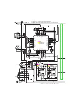
Page 52: ...20 Schematic Diagram for Printing with A4 Size H0211TN HH ...


