background image

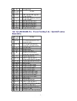
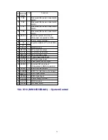
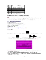
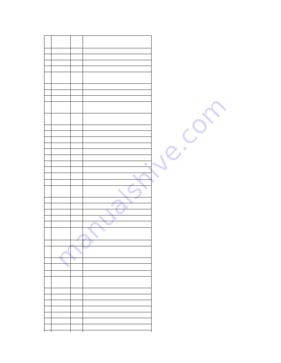
Pin 

No.

Terminal 

Name

I/O

Function

1

CENVD

I

D signal detection input

2

LDO

O

LD amp output terminal

3

APC PD

I

Photo diode detection input

4

LD IN

I

LD amp input

5

APC 

REF

I

APC amp reference voltage input

6 TEMP IN

I

Temperature sensor amp input

7

TEMP

O

Temperature sensor amp output

8

ADIP

O

ADIP FM signal output

9

TOFS

I

Tracking error off-set adjustment 
input

10

TBAL

I

Tracking balance adjustment 
signal input

11

TE

O

Tracking error signal output

12 CRS IN

I

Track cross signal input

13

TGAIN

I

TE gain adjustment input

14

LNP

O

Lens position signal output

15 AB GAIN

I

APP signal gain adjustment input

16

FE

O

Focus error signal output

17 AS GAIN

I

AS gain adjustment input

18

FBAL

I

Focus balance adjustment input

19AS/MON3T O

AS signal output

20

CEA

I

3T envelope detection input

21

BDO/ 

TRCRS

O

BDO/Track cross signal output

22 CBD O

O

BDO detection capacitor terminal

23

OFT O

O

Off-track detection signal output

24

GND

-

GND terminal

25 OFT IN

I

Off-track detection signal input

26

V

CC

I

Power supply terminal

27 NRFDET/ 

OFTR

O

RF detect signal output/Off-track 
signal output

28 NRFLD

I

Serial command latch signal input

29

RF 

DATA

I

Serial command data signal input

30

RFCK

I

Serial command clock signal input

31 NRFSTBY

I

Standby control signal input

32 OUT RF

O

EFM signal output

33

CRF 

AGC

-

RFAGC capacitor connect terminal

34

EQ IN

I

EQ input

35

ARFO

O

RF amp output

36 SVREF

I

Reference signal input

37

VREF

O

Reference voltage output

38

RF1

I

RF 1 signal input

39

RF2

I

RF 2 signal input

40

F1

I

F 1 signal input

41

F2

I

F 2 signal input

30

Summary of Contents for SJ-MD150

Page 1: ...MB0003001C2 Mini Disc Deck SJ MD150 Mechanism Unit MR3A Colour K Black Type Areas E Europe EB Great Britain EG Germany SPECIFICATIONS 1 ...

Page 2: ...Co Ltd All rights reserved Unauthorized copying and distribution is a violation of law 1 Accessories AC power supply cord for E EG areas RJA0043 1C 1 pc AC power supply cord for EB area RJA0044 C 1 pc Optical fiber cable RJL1X009B08 1 pc 2 ...

Page 3: ...c electricity of clothes or human body So be careful of electrostatic breakdown during repair of the MD unit optical pickup 2 1 Handling of MD Unit optical pickup 1 Do not subject the MD unit optical pickup to static electricity as it is extremely sensitive to electrical shock 2 To protect the breakdown of the laser diode an anti static shorting pin is inserted into the flexible board FPC board Re...

Page 4: ...Fig 2 2 Fig 2 2 2 2 2 Work table grounding Put a conductive material sheet or steel sheet on the area where the MD unit optical pickup is placed and ground the sheet Refer to Fig 2 3 Fig 2 3 Caution The static electricity of your clothes will not be grounded through the wrist strap So take care not to let your clothes touch the MD unit optical pickup 3 Precaution of Laser Diode 4 ...

Page 5: ...4 Caution for AC Mains Lead 5 ...

Page 6: ...ipped with a self diagnostic function which in the event of a malfunction automatically display a code indicating the nature of the malfunction Use this self diagnostic function when servicing the unit 6 1 Setting to the self diagnostic function 1 Turn the power ON 6 ...

Page 7: ... the servo processor IC and the microprocessor IC system control Check if the flexible circuit board is disconnected Displayed when the disc is scratched too F28 MD cannot be loaded Confirm that the disc is not catching on anything The connection flexible circuit board or connector cable between the MD unit and th MD servo circuit board is disconnected or damaged check and replace if necessary The...

Page 8: ...ore servicing the unit and check the item as shown below 7 1 Setting to the self check function 1 Turn the power ON 2 With no MD loaded in the unit press and hold the STOP button for at least 2 seconds And then while still pressing the STOP button press the R SEARCH button for at least 2 seconds Then the unit is set to the self check function the FL display is turned off Refer to Fig 7 1 Fig 7 1 7...

Page 9: ...OWER button POWER or pressing and hold the STOP button for at least 2 seconds 8 Operation Checks and Component Replacement Procedures This section describes procedures for checking the operation of the major printed circuit boards and replacing the main components For reassembly after operation checks or replacement reverse the respective procedures Special reassembly procedures are described only...

Page 10: ...10 ...

Page 11: ... Check the main P C B as shown below 8 2 Checking for the FL P C B and operation 1 P C B Follow the Step 1 Step 3 of item 8 1 11 ...

Page 12: ... the FL P C B and operation 1 P C B as shown below 8 3 Removal of the FL P C B operation 1 P C B operation 2 P C B and sensor P C B Follow the Step 1 Step 3 of item 8 1 Follow the Step 1 Step 2 of item 8 2 12 ...

Page 13: ...8 4 Removal of the power switch P C B Follow the Step 1 Step 3 of item 8 1 Follow the Step 1 Step 2 of item 8 2 13 ...

Page 14: ...hecking for the MD servo P C B 8 5 1 Checking for the MD servo P C B A side Follow the Step 1 Step 3 of item 8 1 Check the MD servo P C B A side as shown below 8 5 2 Checking for the MD servo P C B B side 14 ...

Page 15: ...15 ...

Page 16: ...16 ...

Page 17: ... Check the MD servo P C B B side as shown below 17 ...

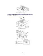
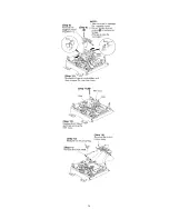
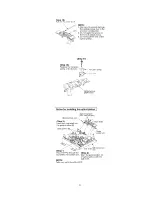
Page 18: ...8 6 Replacement for the magnetic head and optical pickup Follow the Step 1 Step 3 of item 8 1 18 ...

Page 19: ...19 ...

Page 20: ...20 ...

Page 21: ...21 ...

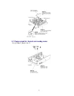
Page 22: ...8 7 Replacement for the belt and loading motor Follow the Step 1 Step 3 of item 8 1 22 ...

Page 23: ...23 ...

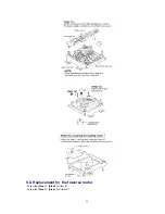
Page 24: ...8 8 Replacement for the traverse motor Follow the Step 1 Step 3 of item 8 1 Follow the Step 1 Step 11 of item 8 7 24 ...

Page 25: ...25 ...

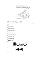
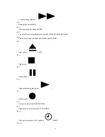
Page 26: ... development of new technology Notes S1 PROTECT det switch S2 REFLECT det switch S3 LOAD OPEN det switch S4 DISC IN det switch S5 LOAD PLAY REC det switch S6 LOAD PLAY det switch S7 LOAD TRG det switch S8 Traverse det switch S251 Unit on off switch I S901 R search switch SEARCH S902 26 ...

Page 27: ...h TRACK MARK CHARA SKIP S906 Display mode select character select switch DISP CHARA S907 Eject switch EJECT S908 Stop switch S909 Pause switch S910 Playback recording start switch S911 Record switch S912 Synchro record switch SYNCHRO REC S913 Playback mode selector switch PLAY MODE S901A Timer selector switch in PLAY position TIMER S902A 27 ...

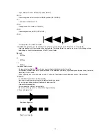
Page 28: ... MD Stop MD Play MD Rec Important safety notice Components identified by mark have special characteristics important for safety Furthermore special parts which have purposes of fire retardant resistors high quality sound capacitors low noise resistors etc are used When replacing any of components be sure to use only manufacturer s specified parts shown in the parts list Caution IC and LSI are sens...

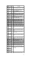
Page 29: ...gnal line 10 Schematic Diagram 11 Printed Circuit Board Diagram 12 Type Illustration of ICs Transistors and Diodes 13 Wiring Connection Diagram 14 Block Diagram 15 Troubleshooting Guide 16 Terminal Function of ICs 16 1 IC1 AN8772FHQ RF Amp 29 ...

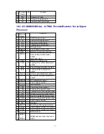
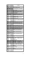
Page 30: ...nput 18 FBAL I Focus balance adjustment input 19AS MON3T O AS signal output 20 CEA I 3T envelope detection input 21 BDO TRCRS O BDO Track cross signal output 22 CBD O O BDO detection capacitor terminal 23 OFT O O Off track detection signal output 24 GND GND terminal 25 OFT IN I Off track detection signal input 26 VCC I Power supply terminal 27 NRFDET OFTR O RF detect signal output Off track signal...

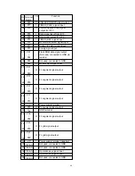
Page 31: ...5 OP I Op amp invert input 6 OP Op amp non invert output Not used connected to GND 7 VCC I Power supply terminal 8 1 2PVCC2 O 1 2PVCC output terminal 2 Connected to GND via capacitor 9 PVCC2 I Power supply terminal for driver 10 PGND2 GND terminal 11 VO4 O Tracking coil drive output 12 VO4 O Tracking coil drive output 13 VO3 O Focus coil drive output 14 VO3 O Focus coil drive output 15 VO2 O Trave...

Page 32: ...justment output 11 FBAL O Focus balance adjustment output 12 TBAL O Tracking balance adjustment output 13 TGAIN O TE error gain adjustment output 14 ASGAIN O Main beam amp gain adjustment output 15 ABGAIN O APP adjustment output 16 AVDD1 I Power supply terminal 17 AVSS1 GND terminal 18 FOD O Focus drive signal output 19 TRD O Tracking drive signal output 20 TVD O Traverse motor drive signal output...

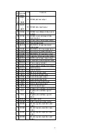
Page 33: ...us signal output 58 DVDD1 I Power supply terminal 59 IVDD1 I Power supply terminal for I O pad 60 DVSS1 GND terminal 61 FS384 O 384 Fs output 62 SCL O Bit clock signal output 63 SWS O Word clock signal output 64 SDAP O Audio data signal output 65 SDAR I Audio data signal input 66 LRCK I CD word clock signal input 67 BCK I CD bit clock signal input 68 DATA I CD data signal input 69 TX O Digital aud...

Page 34: ...O 86 VDSS2 GND terminal 87 RFDAT O RF serial data output 88 RFCK O RF serial clock output 89 NRFLD O RF serial load output 90 TRCRS I Track cross signal input 91 OFTR I Off track signal input 92 APCD O Laser power PWM output 93EXEFMCK I External FM clock input Connected to GND via resistor 94 PEFM1 O EFM loop filter output 95EEMIREF I EFM PLL reference current input 96EEMPLLF O EFM signal output 9...

Page 35: ...Disc in detect switch signal input 14 REFLECT I Reflect detect switch signal input 15LOADSW0 OPEN I Load OPEN detect switch signal input 16LOADSW1 TRG I Load TRG detect switch signal input 17 LOADSW2 PLAY REC I Load PLAY REC detect switch signal input 18LOADSW3 PLAY I Load PLAY detect switch signal input 19PROTECT I PROTECT detect switch signal input 20 MMOD Not used connected to GND 21 RST I Rese...

Page 36: ...30 TEST02 Test terminal Not used open 36 ...

Page 37: ...hronous signal input 45 TEST06 Test terminal Not used open 46 TEST07 I Connected to rec play switch signal 47 TOK OK Test terminal Not used open 48 HF ON O HF module ON signal output 49 PANEL CLK I PANEL I F clock signal input 50 PANEL DATA I I PANEL I F data signal input 51 PANEL DATA O O PANEL I F data signal output 52 PANEL CS O PANEL I F chip select signal output 53 SELAD O MSP MDA I F address...

Page 38: ...erminal 70 VCC5V I Power supply terminal 71 SEL ADDA AD DA converter select signal input Not used open 72 SLOCK Spindle lock output Not used open 73 TLOCK Tracking lock output Not used open 74 FLOCK Focus lock test signal output Not used open 75 ERROR Servo error test signal output Not used open 76 BUSY Servo busy test signal output Not used open 77 SBP RETRY Spindle management retry test signal o...

Page 39: ...No Terminal Name I O Function 1 P97 Not used connected to GND 2 P96 Not used connected to GND 3 P95 O Digital in 1 ON signal output 4 P94 O Digital in 2 ON signal output 5 P93 Not used connected to GND 6 P92 I Chip select signal input 7 P91 O Request signal output 8 P90 O Reset signal output 9 CNVSS O Flash ROM write power supply 10 P87 O LED drive control signal output 11 P86 Not used connected t...

Page 40: ...43 Not used connected to GND 36 P42 I Model select signal input 37 38 P41 P40 O FL segment signal output 39 46 P37 P30 O FL segment signal output 47 54 P27 P20 O FL segment signal output 55 62 P17 P10 O FL segment signal output 63 VCC I Power supply terminal 64 P07 O FL segment signal output 65 VSS GND terminal 66 72 P06 P00 O FL segment signal output 73 80 P57 P50 O FL grid signal output 81 88 P6...

Page 41: ...h music recorded Insulated driver for adjustment such as a ceramic driver Extension cable kit RFKZJMD100EK Remote control transmitter 17 2 Set to the unit to adjustment mode 1 Turn the power ON 2 With no MD loaded in the unit press and hold the STOP button for at least 2 seconds And then while still pressing the STOP button press the F SEARCH button for at least 2 seconds The unit is set to the se...

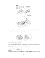
Page 42: ...is tightened too much to deform the resin the position of the head is moved and this affects its recording operation Recommended torque for mounting screw 700 100 g cm Reference This is the same force as using a screwdriver with a 15 mm diameter grip you fasten the screw naturally with your thumb and index finger 3 About the driver for adjusting laser power Use only insulated driver such as a cera...

Page 43: ...er exceeding 600 µ µ µ µW will result in damage to the optical pickup 5 Press 2 on the remote control transmitter WRITE LASER will be displayed to indicate the write power adjustment mode 6 Confirm that the reading of the laser power meter is within the specified range If it is not within the specified range adjust by turning VR1 Refer to Fig 17 5 Specified range write power 4 8 mW 0 1 mW Caution ...

Page 44: ...important for safety Furthermore special parts which have purposes of fire retardant resistors high quality sound capacitors low noise resistors etc are used When replacing any of components be sure to use only manufactures specified parts shown in the parts list The IA IB IC ID marks in Remarks indicate language of instruction manual IA English Spanish Swedish Russian Czech Polish IB English IC G...

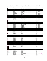
Page 45: ...LAY MODE 1 MAVD 19 RGV0112 S KNOB SLIDE 3 MAVD 20 RGW0308 K KNOB JOG 1 MAVD 21 RGW0310 S KNOB VOLUME 2 MAVD 22 RHD20010 SCREW 1 23 RHD26021 SCREW 14 24 RHD26034 SCREW 3 25 RHN70002 NUT 1 26 RMB0514 SPRING 1 27 RKG0009 MAGNET 1 28 RME0284 SPRING 1 29 XTBR3 20JFZ SCREW 2 30 XTBS3 8JFZ1 SCREW 12 31 XTB3 10JFZ SCREW 3 32 XTB3 8JFZ SCREW 4 101 RHD17021 SCREW 1 102 RHD17022 SCREW 1 103 RMC0348 SPRING 1 ...

Page 46: ...A105ZFV 10V 1U 1 C5 ECUVNA224KBV 10V 0 22U 1 C6 ECUVNA105ZFV 10V 1U 1 C7 C8 ECUVNA224KBV 10V 0 22U 2 C11 ECUVNE223KBV 25V 0 022U 1 C12 ECUV0J474KBV 6 3V 0 47U 1 C13 ECUV1C393KBV 16V 0 039U 1 C14 ECUV1H102KBV 50V 1000P 1 C15 ECST0GY106RR 4V 10U 1 C16 ECUV1H181KV 50V 180P 1 C17 ECUV1H332KBV 50V 3300P 1 C18 ECUV1H562KBV 50V 5600P 1 C19 ECUVNC104ZFV 16V 0 1U 1 C20 ECST0GY106RR 4V 10U 1 C21 ECUV1H822KB...

Page 47: ...0 91 ECUV1H080DCV 50V 8P 2 C92 93 ECUVNC104ZFV 16V 0 1U 2 C94 ECST0GY475RR 4V 4 7U 1 C95 ECUVNC104ZFV 16V 0 1U 1 C96 97 ECST0GY475RR 4V 4 7U 2 C98 ECUVNC104ZFV 16V 0 1U 1 C99 ECUV1H102KBV 50V 1000P 1 C100 ECUVNC104ZFV 16V 0 1U 1 C101 ECST0GY106RR 4V 10U 1 C102 ECUVNC104ZFV 16V 0 1U 1 C103 ECST0GY106RR 4V 10U 1 C106 ECUV1H102KBV 50V 1000P 1 C110 ECUVNC104ZFV 16V 0 1U 1 C111 ECST0GY106RR 4V 10U 1 C1...

Page 48: ...48 ...

Page 49: ...34 ECA0JM102 6 3V 1000U 1 C335 ECEA0JKS470 6 3V 47U 1 C336 ECBT1H104ZF5 50V 0 1U 1 C337 ECBT1C103NS5 16V 0 01U 1 C338 39 ECBT1H104ZF5 50V 0 1U 2 C401 02 ECBT1H104ZF5 50V 0 1U 2 C403 ECBT1H470J5 50V 47P 1 C404 ECBT1H104ZF5 50V 0 1U 1 C502 ECBT1H104ZF5 50V 0 1U 1 C503 ECQV1H224JL3 50V 0 22U 1 C504 ECQB1H223JM3 50V 0 022U 1 C505 ECBT1H102KB5 50V 1000P 1 C506 ECBT1H470J5 50V 47P 1 C507 ECBT1H104ZF5 50...

Page 50: ... CONNECTOR 6P 1 CN401 RJS1A6820 CONNECTOR 20P 1 CN402 RJS2A3330M CONNECTOR 30P 1 CN711 RJS7T4ZA CONNECTOR 7P 1 CN751 RJT029W06VT CONNECTOR 6P 1 CN801 RJS7T7ZA CONNECTOR 7P 1 CN802 RJU057W004 CONNECTOR 4P 1 CN804 RJT029W006 1 CONNECTOR 6P 1 CN901 RJS1A6220 1 CONNECTOR 20P 1 CP6 RJT113W10M CONNECTOR 10P 1 CP802 RJT057W004 1 CONNECTOR 4P 1 D5 D6 SC80209TE12R DIODE 2 D9 MA728TX DIODE 1 D201 MA728TX DI...

Page 51: ... ICP301 SRUN10 IC PROTECTOR 1 JK201 SJS9236 JACK AC INLET 1 JK701 SJF3069 4A IN OUT TERMINAL 1 JK702 GP1F32T OPTICAL OUTPUT 1 JK703 04 GP1F32R OPTICAL INPUT 2 JK801 SJJD17B HEADPHONE JACK 1 L1 RLQU100KT W COIL 1 L2 L3 RLQU101KT W COIL 2 L4 L8 RLQU2R2MT W COIL 5 L9 12 RLQU100KT W COIL 4 L13 14 RLQU2R2MT W COIL 2 L15 RLQU100KT W COIL 1 L201 02 SLQX400 D COIL 2 L501 EXCELDR35V COIL 1 L502 ELEXT5R6KA ...

Page 52: ...450S TRANSISTOR 2 Q901 DTA114ESATP TRANSISTOR 1 MAVD Q902 05 DTC114ESATP TRANSISTOR 4 MAVD Q913 DTC114ESATP TRANSISTOR 1 MAVD R1 ERJ3GEYJ472V 1 16W 4 7K 1 R2 ERJ3GEYJ102V 1 16W 1K 1 R3 ERJ3GEYJ472V 1 16W 4 7K 1 R4 ERJ3GEY0R00V CHIP JUMPER 1 R5 ERJ3GEYJ1R0V 1 16W 1 1 R6 ERJ3GEYJ472V 1 16W 4 7K 1 R8 ERJ3GEYJ271V 1 16W 270 1 R10 ERJ3GEYJ474V 1 16W 470K 1 R11 ERJ3GEYJ101V 1 16W 100 1 R12 ERJ3GEYJ223V ...

Page 53: ...16W 22 2 R73 ERJ3GEYJ393V 1 16W 39K 1 R74 ERJ3GEYJ822V 1 16W 8 2K 1 R75 ERJ3GEYJ223V 1 16W 22K 1 R76 ERJ3GEYJ100V 1 16W 10 1 R77 ERJ3GEYJ223V 1 16W 22K 1 R78 80 ERJ3GEYJ102V 1 16W 1K 3 R81 ERJ3GEYJ223V 1 16W 22K 1 R82 ERJ3GEYJ473V 1 16W 47K 1 R83 ERJ3GEYJ102V 1 16W 1K 1 R84 ERJ3GEYJ153V 1 16W 15K 1 R85 ERJ3GEYJ223V 1 16W 22K 1 R86 87 ERJ3GEYJ102V 1 16W 1K 2 R89 90 ERJ3GEYJ102V 1 16W 1K 2 R93 ERJ3G...

Page 54: ...S2FJ182 1 4W 1 8K 1 R308 ERDS2FJ221 1 4W 220 1 R309 10 ERDS2FJ103 1 4W 10K 2 R311 12 ERD2FCJ4R7 1 4W 4 7 2 R313 14 ERDS2FJ681 1 4W 680 2 R315 16 ERDS2FJ271 1 4W 270 2 R317 18 ERDS2FJ102 1 4W 1K 2 R319 ERDS2FJ681 1 4W 680 1 R320 ERDS2FJ101 1 4W 100 1 R321 ERDS2FJ221 1 4W 220 1 R322 ERDS2FJ101 1 4W 100 1 R323 24 ERDS2FJ222 1 4W 2 2K 2 R325 26 ERDS2FJ103 1 4W 10K 2 R327 ERDS2FJ1R2 1 4W 1 2 1 R401 03 ...

Page 55: ...2FJ182 1 4W 1 8K 1 R918 ERDS2FJ821 1 4W 820 1 R919 ERDS2FJ102 1 4W 1K 1 R920 ERDS2FJ122 1 4W 1 2K 1 R921 ERDS2FJ152 1 4W 1 5K 1 R922 ERDS2FJ182 1 4W 1 8K 1 R923 ERDS2FJ222 1 4W 2 2K 1 R925 ERDS2FJ332 1 4W 3 3K 1 R928 29 ERDS2FJ103 1 4W 10K 2 R932 ERDS2FJ104 1 4W 100K 1 R933 ERDS2FJ101 1 4W 100 1 R934 ERDS2FJ562 1 4W 5 6K 1 R937 ERDS2FJ561 1 4W 560 1 R938 ERDS2FJ471 1 4W 470 1 R940 44 ERDS2FJ103 1 ...

Page 56: ...S LEVEL 1 VR851 EVJY10F01A24 VR PHONES LEVEL 1 VR901 RRV11B152A A VR JOG PUSH SET 1 X1 RSXY10M0M02T OSCILLATOR 1 X2 RSXC16M9S03T OSCILLATOR 1 X901 RSXY10M0M01T OSCILLATOR 1 Z901 RCDGP1U28XD REMOTE SENSOR 1 Z902 EXBZ12E104J COMPONENT COMBINATION 1 Z903 EXBZ8E104J COMPONENT COMBINATION 1 19 Cabinet Parts Location 56 ...

Page 57: ...20 MD Mechanism Unit Parts Location 57 ...

Page 58: ...21 Packaging 58 ...

Page 59: ...F000300000YM KH 59 ...

Page 60: ...DO APC PD LD IN ADIP TBAL TOFS AS MON3T SVREF ARFO EQ IN AGC EQ CRF AGC OUT RF RFDATA NRFLD V CC OFT O B11 26 GND 24 SW 3 tap 3 tap 3T DET VCA VCA 28 SELECT SIGNAL 27 RF BDO COMP AS BDO COMP 20 31 21 COMP COMP 25 22 19 3 tap 17 VCA 4 tap 11 tap FBAL TBAL VCA DARK DET 4 tap DARK DET 4 tap DARK DET 2 3 4 B P F 6 7 VCA 8 9 14 15 16 13 10 42 45 46 48 47 1 VR1 LASER POWER ADJ CLPF2 A B CLPF1 C CENVC D ...

Page 61: ... D01 04 1 2 24 25 30 43 RAD0 12 A0 9 5 9 12 14 18 RAS 4 CAS 23 WE 3 M51V4400D7FS IC72 4M DRAM TC74HCT00AFL IC11 NAND GATE HEAD DRIVE Q10 11 L700 MAGNETIC HEAD B11 ADIP ASGAIN ABGAIN FBAL TOFS TBAL TGAIN FOD TRD TVD SPD AS FE TE LNP SCTSY MDISY FS384 SCL SWS X2 16 9344MHz SGSYNC SSDR SSDW SELAD SSCK APC GEN APCD TS0 3 78 81 MSPMDARST 70 RX1 71 RX2 AVDD0 1 16 98 B11 29 60 DVSS0 1 24 58 83 DVDD0 2 B1...

Page 62: ...46 5 44 10 67 TEST KEY IN TP77 1 2 X1 10 02MHz 33 OSC2 32 OSC1 5 6 TC74HCT7007A IC401 INTERFACE PANEL DATA O 51 31 V DD2 34 37 Vss B10 B10 69 Vcc3V B6 70 Vcc5V 3 4 OPTICAL IN1 D715 D716 B8 B8 Q454 Q455 SELCONT1 SELCONT2 COMMON VOLTAGE MODULATOR L P F 8x INTERPOLATOR MODULATOR L P F 8x INTERPOLATOR SERIAL I O INTERFACE CLOCK DIVIDER 9 16 10 11 12 15 6 21 19 20 1 VRDA B7 2 VRAD 23 VB 24 14 VD VA DGN...

Page 63: ...NTERFACE CLOCK DIVIDER 15 25 11 12 5 28 26 27 7 21 VA DGND 22 8 AGND MCLK MODULATOR MODULATOR 6 3 4 CMODE LRCK SCLK AOUTR AOUTL VCOM VRADR AINR VRADL AINL 14 SDTO 13 SDTI VREFL VREFH 1 2 AK4520AVF E1 IC601 A D D A CONVERTER VD B8 B8 lo MICRO COMPUTER INTERFACE PHASE COMPARATOR PROGRAMMABLE COUNETR LOCK DET SELECT VCO PWDA 23 DEM0 16 DEM1 17 PWAD 24 1 2 4 5 6 7 8 10 9 11 12 13 14 16 15 B8 LOCK V DD...

Page 64: ...Q913 D901 34 P44 33 P45 12 RESET 32 P46 31 P47 DATASP 25 P75 FL901 FL DISPLAY MONO STEREO S903A REC MODE 28 P72 36 P42 37 62 64 66 73 P00 07 10 17 20 27 30 37 40 41 74 83 87 88 P50 57 60 67 B1 Q903 905 X901 10MHz 13 XOUT 15 XIN Z901 REMOTE SENSOR B1 18 P84 B1 B2 16 Vcc 14 Vss B1 99 VREF 97 AVss PLAY OFF REC 23 P77 27 P73 S901A TIMER ANALOG S902A INPUT 30 P70 29 P71 OPT2 OPT1 B1 B3 B1 B3 B1 B3 B1 B...

Page 65: ... BA05ST V5 IC302 BA05ST V5 IC301 B6 BA05ST V5 IC303 B8 D309 310 Q305 D451 D452 B3 Q306 B1 S251 POWER OFF ON OFF ON Q303 D305 308 B2 D323 D324 Q304 Q451 17 P85 AC IN L201 L202 S81233SGY Z IC304 B7 B11 B10 RN5RG33AA TL IC5 RN5RZ26BA TR IC9 Q13 B2 89 VP LED DRIVE P CONT DRIVE FL DRIVE FL DRIVE REGULATOR REGULATOR REGULATOR REGULATOR REGULATOR REGULATOR REGULATOR REGULATOR REGULATOR REGULATOR REGULATO...

Page 66: ...P39 TP52 TP44 TP40 TP57 TP56 TP148 TP150 TP123 TP149 TP38 TP43 TP36 TP41 TP54 TP55 TP101 TP100 TP103 TP110 TP111 TP77 TP74 REP2809A T IC2 IC3 IC4 IC5 IC6 IC9 IC10 IC11 IC92 Q1 Q2 Q3 Q5 Q6 Q13 D201 L2 L3 L4 L5 L6 L7 L9 L10 L11 4D 2D 2B 4C 3D 3C 2C 4B 3B 3F 4E 4F 4C 4C 3B 3B 2D 2D 3E 3E 3B 4B 2B 2B 4B R44 R46 R48 R50 R55 R56 R58 R59 R60 R61 R62 R63 R64 R65 R66 R70 R71 R72 R73 R74 R75 R77 R78 R79 R80...

Page 67: ...112 R114 R115 R116 R117 R121 R122 R124 R125 R130 R131 R132 R134 R135 R143 R201 R212 R213 R215 C1 C7 C8 C41 C42 C45 C51 C52 C53 C57 C59 C60 C61 C64 C65 C71 C72 C84 C85 C86 C90 C91 C93 C94 C95 C96 C97 C99 C100 C101 C102 C103 C110 C111 C112 C114 C115 C117 C122 C129 C133 C138 C140 C141 C142 C143 2J 2J 3K 2J 2I 3L 3K 3L 2H 3K 2K 2K 4K 4J 4K 4J 2K 3J 4J 3H 4H 4H 3H 4H 4J 4H 4H 4H 4H 3L 3K 4I 4I 4I 2H 2L...

Page 68: ...02 C909 W902 2 1 3 4 B C E Q905 B C E Q902 B C E Q901 B C E Q913 B C E Q904 B C E Q903 W901 2 3 1 C912 S912 PLAY MODE S913 SYNCHRO REC X901 C910 FL P C B C S911 S903 EDIT S904 ENTER S905 T MARK CHARA SKIP S901 S902 S908 S909 S910 SEARCH S907 EJECT REP2786A S S7 S8 CN6 IC901 Q901 Q902 Q903 Q904 Q905 Q913 D901 D902 D904 VR901 Z902 Z903 X901 FL901 S901 S902 S903 S904 S905 S906 S907 S908 S909 R918 R91...

Page 69: ... E R L J J J J OUT IN REP2785C M ANALOG DIGITAL OPTICAL Ref No Lo No Ref No Lo No Ref No Lo No R306 R307 R308 R309 R310 R311 R312 R313 R314 R315 R316 R317 R318 R319 R320 R321 R322 R323 R324 R325 R326 R327 R401 R402 R403 R404 R405 R406 R407 R408 R409 R410 R411 R451 R452 R453 R501 R502 R503 R504 R601 R602 R711 R712 R713 R714 R715 R716 R717 R718 R719 R720 R721 R722 R723 R724 R725 R726 R727 R728 R729 ...

Page 70: ...L802 HEADPHONE P C B H PHONES G R L REP2786A S R938 C908 D903 Z901 REMOTE SENSOR W902 2 1 3 1 2 3 4 SENSOR P C B D REP2786A S SENSOR P C B D ELECTRICAL PARTS LOCATION Ref No Lo No Ref No Lo No Ref No Lo No HEADPHONE P C B H OPERATION 1 P C B G D903 W902 Z901 R938 IC801 Q801 Q802 VR801 S901A CN801 CP802 W901 R801 R802 R803 R804 C801 C802 C805 C806 C807 L801 L802 CN802 C803 C804 C808 JK801 R805 R806...

Page 71: ... SWITCH P C B I POWER ON OFF REP2786A S J S902A INPUT ANALOG OPT2 OPT1 MONO STEREO S903A REC MODE VR851 REC LEVEL CN804 W903 3 2 3 4 1 4 5 6 2 1 J OPERATION 2 P C B F REP2786A S ELECTRICAL PARTS LOCATION OPERATION 2 P C B F Ref No Lo No Ref No Lo No POWER SWITCH P C B I POWER TRANSFORMER P C B J CN804 W903 CN251 JK201 T201 R201A VR851 S902A S903A S251 L201 L202 CN201 W201 2C 2B 3E 5B 7C 8D 2C 2B 2...

Page 72: ...PD GND VREF RF2 RF1 D C Vcc B F2 F1 A LD LD GND H G I J K L F 0 1 1 F PD 0 022 300 C D E P 1 2 3 4 5 6 7 14 13 12 11 10 9 8 GND Vcc C5 0 22 R6 4 7K R8 270 R5 1 C6 1 C123 0 1 C117 6 3V330 R29 47K R30 1K TP35 TP37 TP44 C8 0 22 C7 0 22 C1 220P R1 4 7K R3 4 7K R72 22 C133 1 C60 16V10 D6 SC80209TE12R TP110 R13 3 3 TP111 C81 56P C120 56P C118 1 Q R S T U V W I L K J R77 22K R75 22K R73 39K C106 1000P R7...

Page 73: ...8 C14 1000P C13 0 039 C122 1 C12 0 47 R43 2 2K TP52 R S T U V W Q P C C129 100P R25 100K R16 100K TH1 10K C86 0 015 R15 22K C24 1000P C26 4700P C67 3900P R84 15K R82 47K C61 0 33 R34 2 7K C25 0 039 TP55 R23 2 7K R20 47K R19 1K C65 0 1 R10 470K C11 0 022 R14 10K L K I H F G N M J R18 10K C66 0 082 TP123 TP149 TP150 TP122 TP36 TP38 TP43 TP42 TP40 TP39 TP41 TP56 TP54 R49 0 L1 10 H SCHEMATIC DIAGRAM 2...

Page 74: ... LOAD1 MSP RST PC NRF STBY AD RST MUTE DEO DAC RST RST SPMWE G H I J K L M N O Q R C121 1000P C99 1000P R81 22K R110 1K R67 1K R124 47K R125 47K R114 10K R115 10K C115 560P C114 560P C119 1000P TP77 C141 0 1 C142 0 1 C112 16V10 R56 22K D E F G H I J K L R98 1K R93 1K R103 1K R90 1K R89 1K R99 1K R80 1K R70 1K R135 2 7K R104 2 7K R105 2 7K R121 2 7K R122 2 7K R134 2 7K R132 2 7K R130 2 7K C113 0 1 ...

Page 75: ...6 3V330 TP103 TP100 TP101 Q6 DTC114YETL POWER SUPPLY CONTROL R131 100 R11 100 R117 100 R116 100 C72 0 1 C71 0 1 C85 4V10 26 25 24 23 22 18 17 16 15 14 1 2 3 4 5 9 10 11 12 13 DO1 DO2 WE RAS A9 A0 A1 A2 A3 Vcc Vss DO4 DO3 CAS OE A8 A7 A6 A5 A4 L3 100 H SCHEMATIC DIAGRAM 4 5V 5V 3 3V 2 6V 2 5V 2 5V 2 5V 2 5V 0V 5V 2 5V 1 3V 1 3V 3 3V 1 3V 3 3V 1 3V 1 3V 0V 0V 0V 0V 2 5V 2 5V 2 5V 2 5V 0V 0V 5V 5V 2 ...

Page 76: ...33 4V10 A B C D E F G H I J K L M N O P Q R C N L F I G Q D J E O K M R B R12 22K C22 1000P C70 0 012 R47 47K R50 1K C82 0 047 C62 220P R58 6 8K R59 68K S C83 0 1 C139 0 1 C111 4V10 C80 0 1 C73 0 1 C15 4V10 IC9 RN5RZ26BA TR REGULATOR A W H V T U P C A L5 2 2 H L2 100 H L4 2 2 H R48 0 R143 0 MD SERVO CIRCUIT SCHEMATIC DIAGRAM 5 C110 0 1 C58 1000P 5V 2 6V 3 3V 3 3V 2 6V 2 6V 3 3V 3 3V 0V 0V 3 3V 3 3...

Page 77: ... TL REGULATOR IC4 AK4518VF E2 AD DA CONVERTER DEO DA GND SDAP A 3 3V SDAR SCL M GND M GND SWS LOAD SW NC D GND HEAD 5V SYSRST DATAO DATAI CLK CS REQ RX2 RX1 LED3 TX LED1 KEY2 KEY1 VREF M 5V D 3 3V L 5V A D C E R21 22K R31 22K R66 470 R65 470 C100 0 1 U V T W Q C140 0 1 C154 33P R95 2 2K C155 33P R145 220 R146 220 C75 0 1 R201 4 7K D201 MA728TX C Q R210 390 R213 100 R212 390 R215 390 R211 100 L14 2...

Page 78: ...7 560 R940 10K D902 SLR325MCT31 JOG PUSH SET R906 4 7K R925 3 3K R923 2 2K R922 1 8K R921 1 5K R920 1 2K R919 1K R918 820 R913 820 R914 1K R915 1 2K R916 1 5K R917 1 8K R907 2 2K S913 PLAY MODE S912 SYNCHRO REC S910 S909 S908 S901 SEARCH S902 SEARCH S903 EDIT S904 ENTER S905 TRACK MARK CHARA SKIP S906 DISP CHARA FL DISPLAY 11 21 31 41 51 12 22 32 42 52 13 23 33 43 53 14 24 34 44 54 15 25 35 45 55 ...

Page 79: ...REF P51 P52 P53 P54 P55 P56 P57 P00 P01 P02 P03 P04 P05 P06 P07 P10 P11 P12 P13 P14 P15 P16 P17 P20 P21 P22 V SS V CC P25 P26 P27 P30 P31 P32 P33 P34 P35 P36 P37 P40 P41 P42 P43 P44 P45 P46 P97 P96 P95 P94 P93 P92 P91 P90 CNV SS P87 P86 RESET V SS XOUT XIN V CC P85 P84 P83 P82 P81 P80 P77 P76 P75 P74 P73 P72 P71 P70 P50 P23 P24 P47 1 2 3 4 5 6 7 8 9 10 11 12 13 14 15 16 17 18 19 20 1 2 3 4 5 6 7 8...

Page 80: ... M GND SCL SDAR A 3 3V SDAP DA GND DEO NC LED1 KEY2 KEY1 1 2 3 1 2 3 D715 1SS254TA D716 1SS254TA R761 2 2K C764 0 1 C765 0 1 C766 25V4 7 C767 25V4 7 D453 1SS254TA D454 1SS254TA C336 0 1 C335 6 3V47 C763 0 1 C334 6 3V1000 C401 0 1 C402 0 1 D318 1SS291TA D317 1SS291TA R408 270 C403 47P R403 10K R401 10K R402 10K R405 10K R406 270 R407 1K R404 270 R409 1K R410 1K R411 1K GND VCC NC NC 1 2 3 4 5 6 7 8...

Page 81: ... 4 5 6 7 8 9 10 11 12 13 14 15 16 17 18 19 20 21 22 23 24 25 LPF LPF COMMON VOLTAGE MODULATOR MODULATOR DECIMATION FILTER DECIMATION FILTER VA AGND SERIAL I O INTERFACE MODULATOR 8X INTERPOLATOR 8X INTERPOLATOR MODULATOR CLOCK DIVIDER DGND VD TST1 TST2 TST3 DEM1 DEM0 PWDA PWAD 28 26 27 L502 5 6 H SCHEMATIC DIAGRAM 10 5V 5V 5V 5V 2 4V 2 3V 5V 2 6V 2 6V 5V 5V 5V 1 6V 1 4V 4 9V 2 5V 2 5V 2 5V 5V 4 8V...

Page 82: ... 1SS254TA D323 1D3 E R315 270 R313 680 R311 1 4W4 7 D309 1D3 E C311 25V470 C313 0 1 D311 MA4091MTA ICP301 SRUN10T C312 25V470 C309 0 1 C314 0 1 R312 1 4W4 7 R310 10K R314 680 D310 1D3 E R316 270 C316 25V47 D324 1D3 E C318 10V220 R452 10K Q451 2SD1862QRTV6 REGULATOR R451 10K Q306 2SB1240QRTV6 REGULATOR R724 150K R726 330 C720 25V47 R722 33K R720 33K C718 390P C716 390P R718 12K R716 8 2K C714 1000P...

Page 83: ... 50V22 R309 10K R307 1 8K R308 220 C307 1000P D308 MA4270HTA D305 307 1D3 E C806 0 01 C805 0 01 R801 68 R802 68 R804 2 2K R803 2 2K N C802 10V100 N C801 10V100 C807 0 01 N C758 25V3 3 R760 470 C756 2 2P R758 220K R756 33K R754 27K N C754 25V3 3 N C757 25V3 3 R759 470 C755 2 2P R755 33K R757 220K R753 27K N C753 25V3 3 1 2 3 4 5 6 OFF ON OPT2 OPT1 MONO STEREO 5 6 7 8 1 2 3 4 G J I H F L802 3 3 H L8...

Page 84: ...2SB1121ST TD C B E 2SJ278MYTR 2SK1764KYTR D G S 2SB1295 6 TB 2SB1462STX DTC114YETL E C B M30218MAA102 50 51 1 30 31 100 80 81 BA05ST V5 1 5 2SD1450RSTTA E C B SC80209TE12R A Ca Anode Cathode MA4051MTA MA4056MTA MA4062MTA MA4091MTA 2SD2037EFTA E C B DTA114ESATP DTA143ESATP DTC114ESATP E C B Anode Cathode MA304TX A Ca 1D3 E A Ca 1SS254TA A Ca SLR325MCT31 SLR325VCT31 A Ca MA4270HTA Cathode Anode Anod...

Page 85: ...B SWITCH P C B CN6 MD OPTICAL PICKUP 26 1 MAGNETIC HEAD 1 29 2 30 CN402 6 1 CN301 1 6 W201 T201 POWER TRANSFORMER AC IN 1 4 CN201 4 1 CN251 6 1 CN751 ANALOG 20 2 19 1 CN401 7 1 CN711 6 1 PINK WHITE BLACK BLACK WHITE PINK PINK WHITE BLACK BLACK WHITE PINK 6 1 6 1 CN804 4 1 W903 1 4 W903 CN901 PHONES 4 1 1 4 CP802 CN802 CN801 W902 W901 1 4 W902 W901 GRAY GRAY 30 2 29 1 2 6 1 5 10 1 10 1 1 3 1 7 3 1 ...

Page 86: ...and check ROM data laser power and RAM data laser power To ROM RAM Operation Is CN4 power supply line OK Is oscillation signal input for IC10 pin 32 Check power supply circuit on main unit Faulty IC10 Is IC10 pin 21 H 1 Continued on next page 2 O U S T 5V 5V 5V 3 3V 3 3V CN4 Check reset circuit on main unit NO YES NO YES NO YES NO YES NO YES NO YES NO YES NO YES Continued on next page Is CN4 pin 1...

Page 87: ...times value indicated on pick FPC 2 2 YES NO Is output of IC3 pin 92 OK Is voltage of IC1 pin 2 left side of R8 approx 1 9 V 1 NO YES NO YES NO YES 3 3V 0V 3 3V 0V NO YES NO YES 2 Indicated value Current equal to that on both sides of R5 divided by 1 Faulty IC1 Is voltage of IC9 pin 3 2 6 V YES Faulty L5 Faulty IC9 NO NO Faulty IC3 Faulty IC1 Faulty optical pickup For measurements of IC1 refer to ...

Page 88: ...H L H 3 3V L 0V 5 NO IC3 pin 21 Faulty IC3 Faulty IC2 Does optical pickup move up and down Continued on next page Does CN4 pin 18 change from H to L when disc is inserted Faulty loading TRG S7 D i s c t r a y O P E N L H H H Is output of IC10 pins 13 15 17 and 18 OK Is voltage of IC10 pins 8 and 9 OK Is voltage output from IC92 pins 2 and 4 Faulty loading motor Faulty S3 S4 S5 and S6 Faulty IC10 F...

Page 89: ...tput from IC1 pin 32 TP52 1 Is there output from IC1 pin 29 TP148 or IC3 pin 87 1 IC1 pin 29 TP148 or IC3 pin 87 Is RF signal stable Are communications between IC3 and IC72 OK Communications error Is voltage output from IC3 pin 96 Faulty IC1 Faulty IC1 Faulty IC3 Faulty IC72 Is voltage output from IC1 pins 38 TP44 and 39 TP37 1 Faulty optical pickup Continued on next page For measurements of IC1 r...

Page 90: ...Operation complete Faulty magnetic head Faulty magnetic head Is shape of magnetic head OK Is there output from CN8 TP110 and TP111 Is output of IC3 pin 73 OK Faulty magnetic head circuit Faulty IC3 Is output of IC3 pins 61 65 OK during playback Faulty audio circuit Faulty IC3 To two pages before After TOC is read does traverse move to UTOC Faulty IC1 See Traverse Operation next page F 16 9344MHz 3...

Page 91: ...ner track Remains at outer track Is IC10 pin 12 approx 3 3 V Faulty traverse detection switch S8 Is IC10 pin 12 approx 0 V Faulty shorted traverse detection switch S8 or Is output of IC3 pin 20 OK Is voltage output between IC2 pins 15 and 16 Faulty IC2 Faulty IC3 Faulty traverse motor ...

Page 92: ...LEVEL Timer selector TIMER Display Record button Stop button Pause button Playback mode selector PLAY MODE Synchro record button SYNCHRO REC E Playback recoding start button F Recording level control REC LEVEL G Recording mode selector REC MODE H Input selector INPUT Panel open button PUSH OPEN Press this button to open the transparent panel Close the panel by hand No Name No Name A B C D Front pa...

Reviews: