


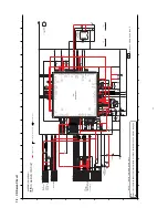


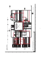


SA-AKX14
POWER SUPPL
Y
(2/2) BLOCK DIAGRAM
TO POWER SUPPLY
BLOCK (1/2)
1
3
2
4
14
4
CN6001
CN2003
SYS3.3V
DVREF+
SYS3.3V,DVREF+
DVREF+
DVREF+
CD+7.5V
CD+7.5V
+7.5V
+7.5V
3.3V
3.3V
3.3V
SYS3.3V
SYS3.3V
VREF+
VREF+
VREF+
D2018,D2019
D2020,D2021
DVREF
12
6
CN6001
CN2003
3.3V
5
5
CN51
CN2010
3.3V
CD 3.3V
CD 3.3V
CD3.3V
CD3.3V
10
8
CN6001
CN2003
3.3V
2
2
CN6006
CN6005
3
3
CN6000
ZJ6002*
+5V
+5V
CD3.3V
+5V
+5V
CD3.3V
+5V
16
2
CN6001
CN2003
5V
1
1
CN6000
ZJ6002*
VBUS
4,5
2
ZJ6001*
CN7901
4
CN2001
4,5
CN2005
3.3V
1
27
CN7002
CN2706
7.5V
+5V
+5V
+5V
5V
15,16
12,13
CN7002
CN2706
5V
VBUS
VBUS
VBUS
CD 3.3V
3.3V
3.3V
22
6
CN7002
CN2706
3.3V
LD SW
LD SW
LD SW
13
15
CN7002
CN2706
LDSW
PANEL P.C.B.
REMOTE SENSOR P.C.B.
CD SERVO P.C.B.
TUNER P.C.B.
USB P.C.B.
MAIN P.C.B.
LCD P.C.B.
72
Summary of Contents for SA-AKX14LM-K
Page 14: ...5 General Introduction 5 1 Media Information 14 ...
Page 15: ...6 Location of Controls and Components 6 1 Remote Control Key Button Operation 15 ...
Page 16: ...6 2 Main Unit Key Button Operation 16 ...
Page 17: ...7 Installation Instructions 7 1 Speaker and A C Connection 17 ...
Page 28: ... 3 D Amp IC Operation Control 28 ...
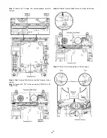
Page 33: ...11 2 Main Components and P C B Locations 33 ...
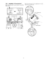
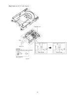
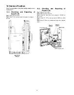
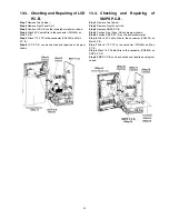
Page 63: ...Step 9 Ground the 24P FFC with a short pin 63 ...
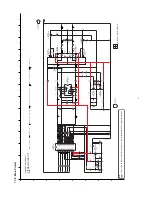
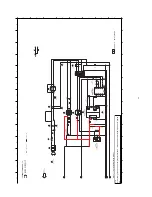
Page 67: ...14 Simplified Block Diagram 14 1 Overall Simplified Block Diagram 67 ...
Page 68: ...14 2 Power Block Diagram 68 ...