background image

22

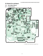
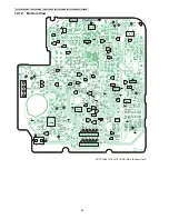
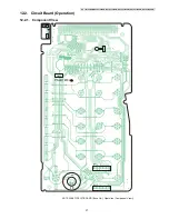
KX-TS2388RUB/KX-TS2388RUW/KX-TS2388CAB/KX-TS2388CAW/KX-TS2388UAB/KX-TS2388UAW

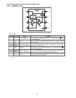
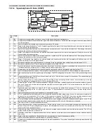
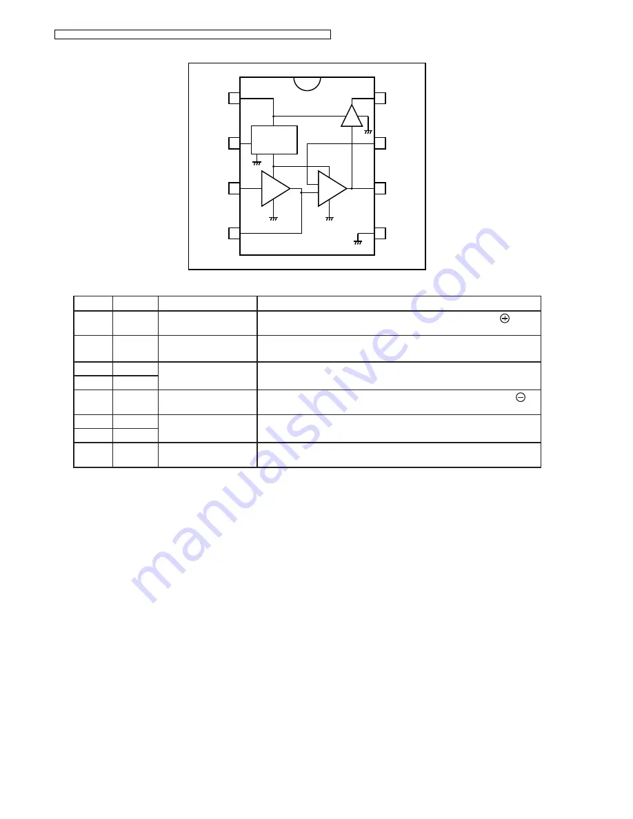
10.1.2. RINGER IC (IC1)

Vcc 1

R

S

L 2

LFI

3

LFO 4

OUT

8

HFI

7

HFO

6

GND

5

LOW FREQ
O

S

C

HIGH FREQ
O

S

C

POWER 

S

UPPLY

WITH

HY

S

TERI

S

I

S

AMP

Pin de

s

cription

s

1

2

3

4

5

6

7

8

Vcc

R

S

L

LFI

LFO

GND

HFO

HFI

OUT

Pin No. Pin name

Power 

su

pply pin

R

S

L pin

Low-fre

qu

ency time

con

s

t

a

nt connector pin

GND pin

High-fre

qu

ency time

con

s

t

a

nt connector pin

O

u

tp

u

t pin

Thi

s

 i

s

 the power 

su

pply pin for the lC. It i

s

 connected to the (     ) pin of

 the diode 

b

ridge.

Thi

s

 i

s


us

ed to ch

a

nge the oper

a

tion initi

a

tion c

u

rrent when connected 

to the GND pin.

Thi

s

 i

s

 connected to the time con

s

t

a

nt th

a

t determine

s

 the o

s

cill

a

tion 

fre

qu

ency on the w

a

r

b

le. 

Thi

s

 pin h

as

 the lowe

s

t potenti

a

l on the lC. It i

s

 connected to the (     )

pin of the diode 

b

ridge.

Thi

s

 i

s

 connected to the time con

s

t

a

nt th

a

t determine

s

 the o

s

cill

a

tion 

fre

qu

ency on the tone 

s

ide (the 

au

di

b

le fre

qu

ency 

s

ide).

Thi

s

 i

s


us

ed to connect 

a

 piezoelectric 

bu

zzer, or to connect 

a

 dyn

a

mic 

s

pe

a

ker thro

u

gh 

a

 tr

a

n

s

former.

Name

Function

Summary of Contents for KX-TS2388RUB

Page 1: ...nd distribution is a violation of law ORDER NO KM41010283CE Telephone Equipment Model No KX TS2388RUB KX TS2388RUW KX TS2388CAB KX TS2388CAW KX TS2388UAB KX TS2388UAW Integrated Telephone System B Black Version W White Version for Russia Central Asia and Ukraine ...

Page 2: ... by in the Schematic Diagrams Circuit Board Diagrams Exploded Views and Replacement Parts List It is essential that these critical parts should be replaced with manufacturer s specified parts to prevent shock fire or other hazards Do not modify the original design without permission of manufacturer IMPORTANT INFORMATION ABOUT LEAD FREE PbF SOLDERING If lead free solder was used in the manufacture ...

Page 3: ...ervice Hints 13 8 2 Pulse Dialing Problems 13 8 3 Tone Dialing Problems 14 8 4 No Ringing Sound When Ring Signal is Input 14 9 Disassembly and Assembly Instructions 15 9 1 Disassembly Instructions 15 9 2 Assembly Instruction 17 10 Miscellaneous 21 10 1 IC Block diagram 21 10 2 How to Replace the Flat Package IC 25 10 3 Terminal Guide of the ICs Transistors and Diodes 27 11 Schematic Diagram 28 11 ...

Page 4: ...ufacturer 3 Dispose of used batteries according to the manufacturer s Instructions 2 2 About Lead Free Solder Pbf Pb free Note In the information below Pb the symbol for lead in the periodic table of elements will refer to standard solder or solder that con tains lead We will use PbF solder when discussing the lead free solder used in our manufacturing process which is made from Tin Sn Silver Ag a...

Page 5: ...nc and Bismuth Sn Zn Bi Please check the manufac turer s specific instructions for the melting points of their products and any precautions for using their product with other materi als The following lead free PbF solder wire sizes are recommended for service of this product 0 3 mm 0 6 mm and 1 0 mm 2 3 Discarding of P C Board When discarding P C Board delete all personal information such as telep...

Page 6: ... UM 3 batteries Memory Capacity 50 Caller ID memory 50 Directory memory Redial The unit redials the last dialed number Microphone Electret condenser microphone Input Jack Telephone Line Approx 93 mm x 172 mm x 220 mm Dimensions H x W x D Mass weight Approx 550 Operating Enviroment 0 o C 40 o C 20 80 relative air humidity dry g Speaker Unit Unit 5 7cm 2 5 PM magnetic type 32 Handset 3 cm 113 16 PM ...

Page 7: ... Q501 Q502 Battery LCD KX TS880 TS2388 Series BLOCK DIAGRAM Q422 Q401 Q402 Q403 IC801 MICON Ringer indication LED LED1 Small PCB JOHN SMITH 1234567890 RINGER IC INUSE EXHOOK Line ON OFF Handset Receiving Amp EEPROM 128K TIPIN Sidetone Bridge RESET BATTLOW Reset IC 2 7V Handset Sending Amp Keyboard Switch RINGIN Battery Low Detector Regulator 3 3 V FSK DTMF Circuit Wakeup Circuit WAKEUP Dummy Ringe...

Page 8: ...e will be activated during dummy ring IC801 pin 89 R901 Q2 SW2 R11 R12 R13 C8 R615 C616 IC601 pin 19 IC601 pin 15 C618 Speaker 4 2 3 Telephone Line Interface 4 2 3 1 Circuit operation On hook Q101 is OFF on hook condition where DC loop is disconnected and voice signal flow is cut Off hook During Off Hook pin 1_3 of SW101 and Q101 is ON providing an off hook condition active DC current flow through...

Page 9: ...ttenuator Control corresponding to the RX sig nal The Attenuator Control provides a control signal to the TX and the RX attenuator to switch the appropriate signals on and off The Attenuator Control also detects the level of the volume control to automatically adjust for changing ambient conditions 1 Transmission signal path The input signal from the microphone is sent through the circuit via the ...

Page 10: ...the batteries is inserted into the unit then the voltage is regulated by IC302 and power is supplied to the CPU The set can operate in the circuit voltage diagram Regulator 1AP PCB Reset Circuit 2AP PCB IC302 1 VIN 2 GND 4 NC 5 VOUT 3 STBY C301 Battery 4 5V C302 C304 C303 D301 C864 IC861 1 VOUT 2 VCC 3 NC 4 GND Q862 VCC R863 R862 R833 R864 C862 Stop Reset Vcc IC801 105 3 3 V 3 3 V 3 3 V IC801 81 I...

Page 11: ...ll signal The data from the telephone exchange is a modem signal which is modulated in an FSK Frequency Shift Keying format Data 0 is a 1200 Hz sine wave and data 1 a 2200 Hz sine wave There are two types of the message for mat which can be received i e the single message format and plural message format The plural message format allows to trans mit the name and data code information in addition t...

Page 12: ...erating Instructions Note You can download and refer to the Operating Instructions Instruction book on TSN Server 7 Operating Instructions Refer to the Operating Instructions Note You can download and refer to the Operating Instructions Instruction book on TSN Server 7 1 For Service Hint If the current password is forgotten key in 7000 then ENTER at the change password menu and you will be able to...

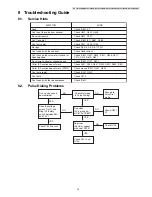
Page 13: ...volume for Handset or Speakerphone Check IC801 Q107 Q401 No volume handset or speakerphone SYMPTOM CURE Check C551 C552 R551 R552 D551 D554 IC801 Caller ID Function doesn t work Check around IC501 Q501 Q502 Caller ID Function doesn t work DTMF Check IC201 Q201 Can t auto redial Check Q110 Can t hold Check IC601 Can t speak with the speakerphone Can a pulse sound be monitored Check TEL line Jack Do...
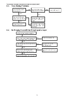
Page 14: ...07 Check C485 R487 R490 C415 L411 L409 and Q403 Check R481 R485 R486 R488 C483 VR481 L421 and R430 NO Check IC801 and X1 NO YES Is the voltage across Pin 8 and Pin 2 of Check the telephone line Check C1 R1 R2 D1 D3 D6 and LED1 Does a sine wave of approximately 60V or more appear across Tip and Ring YES NO YES Call the unit from another telephone Does the tone ringer output signal appear across Pin...

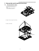
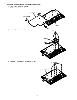
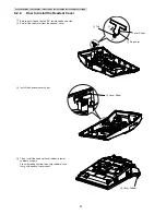
Page 15: ...ly Instructions 9 1 Disassembly Instructions 1 Press the catches 1 and rotate the stand in the direction 2 to remove the Stand Note When the Stand is in Low position the screws can be taken out just as it is 2 Remove 5 Screws to remove the Cabinet Cover 3 Remove the Hook Button 1 2 3 Hook Button 2 5 Screws ...

Page 16: ...UAW 4 Rem LED P C Board and Tel Line Jack ove Main P C Board then unhook the 5 Remove the 3 screws to remove the speaker LED P C Board Main P C Board Speaker 3 screws Speaker Operation P C Board 5 Tel Line Jack 6 Remove the 4 screws to remove the Operational P C Board 4 screws 6 ...

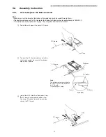
Page 17: ...ed in this page They may differ from the actual product Peel off the arak tape at the front of P C board P C board Arak Tape 1 Peel off the HSC Heat Seal Connector from the P C board in the direction of the arrow Use some IPA alcohol to gently remove glue stain on the P C board P C board LCD 3 2 P C board P C board Platform Platform Crystal Side View Note The platform height must be able to protec...

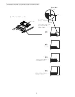
Page 18: ...tseal of the new LCD New LCD 0 2 mm 0 2 mm Horizontal Interval Tolerance Vertical Interval Tolerance OK NG NG NG Horizontal interval tolerance is more than 0 2 mm Vertical interval tolerance is more than 0 2 mm Inclined If interval tolerance between center lines is less than 0 2 mm it is o k 4 ...

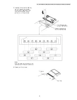
Page 19: ...g iron for 10 seconds each position in case of 60W soldering iron with 10kg pressure applied 9 times on position A I as shown below Replace back the arak tape 6 Note Make sure copper part of solder jig is not touch the new LCD which will cause burn Rubber of Soldering Iron Part No PQZZ430PRB Tip of Soldering Iron Part No PQZZ430PIR 5 P C board Arak Tape ...

Page 20: ...ll the headset cover rubber to lower cabinet as shown Press the rubber harder to ensure rubber attach firmly with headset cover sheet Separator 90 Cover Sheet Tab Install the headset cover sheet Before install bend the tab 90 towards adhesive side Peel off the separator from the headset cover 2 3 4 1 2 Cover Sheet 3 4 Cover Rubber 2 ...

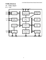
Page 21: ...6 bit Processor RAM 2k x 16 Sleep INT Control OTPROM 36k x 16 Time Base Gen 8 bit timer x 1 16 bit timer x 1 32768Hz XTAL OSC RC OSC XTAL OSC System Clock Gen Max 16 x 56 LCD Driver PGA Pre Amp 10 bit SARADC Signal Channel 8 bit DAC Output 32 IO Ports 31768Hz ROSC IOA 7 0 IOB 7 0 IOC 7 0 IOD 7 0 DTMFO DAC2 PGAIN PGAIN2 GS TIPIN RINGIN RESET COM 15 0 SEG 55 0 XI XO X32I X32O ...

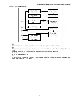
Page 22: ... Output pin This is the power supply pin for the lC It is connected to the pin of the diode bridge This is used to change the operation initiation current when connected to the GND pin This is connected to the time constant that determines the oscillation frequency on the warble This pin has the lowest potential on the lC It is connected to the pin of the diode bridge This is connected to the time...

Page 23: ...e pull up resistance external because output circuit of SDA uses Open Drain 3 A0 A1 A2 A0 A1 and A2 terminal is not used 4 WP WP terminal controls writing action It is possible to do only reading action when high level input and it is possible to do read ing and writing action when low level input Dout ACK Open drain Control logic Sense amps Shift resistor Word address buffers Column decorders Sta...

Page 24: ... used to prevent loading ac line sig nals The required V voltage is 6 0 to 11 V 7 5 V nominal at 7 0 mA 17 AGC A capacitor from this pin to VB stabilizes the speaker amp gain control loop and additionally controls the attack and decay time of this circuit The gain control loop limits the speaker amp input to prevent clipping at SKO The internal resistance at the AGC pin is nominally 110 kohms 18 C...

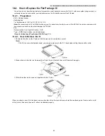
Page 25: ...could overheat and damage the PCB foil Flux Recommended Flux Specific Gravity 0 82 Type RMA lower residue non cleaning type Note See About Lead Free Solder Pbf Pb free P 4 10 2 2 How to Remove the IC 1 Put plenty of solder on the IC pins so that the pins can be completely covered Note If the IC pins are not soldered enough you may give pressure to the P C board when cutting the pins with a cutter ...

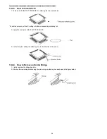
Page 26: ...pins Check the accuracy of the IC setting with the corresponding soldering foil 2 Apply flux to all pins of the FLAT PACKAGE IC 3 Solder the pins sliding the soldering iron in the direction of the arrow 10 2 4 How to Remove a Solder Bridge 1 Lightly resolder the bridged portion 2 Remove the remaining solder along the pins using a soldering iron as shown in the figure below ...

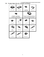
Page 27: ...TBF822T7 B1GBJCFJ0003 B1GBJCJJ0003 UNR5113J0L 2SD1819KSL 2SB1218KSL 8 5 4 1 C1CB00002903 C0ABBA000025 PQVINJU7014R PNWITS2388RU PNWITS2388CA PNWITS2388UA MA111 MA728 Cathode Anode B1AAKD000013 1 3 5 4 PQVIPS3238NT C0DBZGC00067 1 3 2 4 PQVIPS3327UT C2CBYY000895 97 128 1 32 33 64 65 96 C1CB00001673 1 14 15 28 E C B Cathode Anode MA4051 Cathode Anode B0JCME000038 1 8 16 9 C0ZBZ0001747 E C B 2SA1776P ...

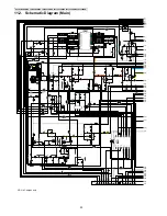
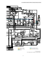
Page 28: ...AW KX TS2388UAB KX TS2388UAW 11 Schematic Diagram 11 1 For Schematic Diagram 1 DC voltage measurements are takens with electronic voltmeter from negative terminal 2 This schematic diagram may be modified at any time with the development of new technology ...

Page 29: ...29 KX TS2388RUB KX TS2388RUW KX TS2388CAB KX TS2388CAW KX TS2388UAB KX TS2388UAW Memo ...

Page 30: ...33 u C485 0 01 u C483 1500p C486 100p C422 6800p C424 1800p C426 100p C429 0 1 u C8 0 1 u C9 NC C412 0 1 u C413 0 1 u C414 0 1 u C610 1u C611 1u C624 NC C481 1000p C432 0 015 u C117 C482 1000p C600 NC R116 270 R404 56 R401 1k R411 2 2 k R185 NC R119 15 R416 NC R606 30k R607 68k R605 2 2 M R608 4 7 k R609 2 7 M R603 3 3 k R604 4 7 k R600 3 3 k R601 10K R610 100k R611 18k R612 1 8 k R613 100k R614 4...

Page 31: ...3 330p C554 1000p C116 NC C1 1u 250 C200 NC C300 NC C100 NC R106 390K R180 0 R182 1 8 k R181 NC R183 NC R184 NC R109 NC R112 220 R114 NC R115 10k R102 NC R105 180k R12 9 N C R101 NC R131 NC R121 3 3 M R204 390k R205 5 6 k R203 10k R207 10k R206 18k R202 120k R20 8 4 7 k R622 10k R201 10k R654 NC R655 NC R3 27k R 4 330k R6 NC R522 180k R502 180k R506 1 2 k R508 3 3 M R507 330k R509 27k R510 390k R5...

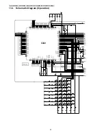
Page 32: ... DTMFO 92 TIPIN 93 RINGIN 94 NC16 95 NC17 96 NC18 97 NC19 98 NC20 99 NC21 100 G S 101 PGAI N 102 PGAIN2 103 VR2 104 AVDD 105 LVDD 2 106 COM 0 107 COM 1 108 COM 2 109 COM 3 110 COM 4 111 COM 5 112 COM 6 113 COM 7 114 COM 8 115 COM 9 116 COM1 0 117 COM1 1 118 COM1 2 119 COM1 3 120 COM1 4 121 COM1 5 122 SEG 0 123 SEG 1 124 SEG 2 125 SEG 3 126 NC22 127 NC23 128 NC24 1 NC1 2 NC2 3 NC3 4 SEG4 5 SEG5 6 S...

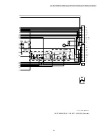
Page 33: ...M TP14 BATTP TP18 INUSE TP26 TXMUT E TP13 HOOK TP17 TON E TP19 RXMUTE TP15 ACKMUTE TP27 WAKEUP TP20 CIDW TP30 RING TP29 TI P TP24 MUSIC DTMF TP23 BEEP DRING TP832 TP833 TP16 PULSE TP22 MIC TP21 MIC TP12 VSS TP28 VDD PCB TP11 SDA TP25 SCL TP862 D861 IC831 1 A0 2 A1 3 A2 4 VSS 5 SDA 6 SCL 7 WP 8 VCC SMALL PCB Battery Out Reset Circuit CN2 CN1 Battery Low KX TS2388RU UA CA SCHEMATIC DIAGRAM Operation...

Page 34: ...34 KX TS2388RUB KX TS2388RUW KX TS2388CAB KX TS2388CAW KX TS2388UAB KX TS2388UAW Memo ...

Page 35: ...R6 R104 R105 JP101 D105 Q105 JP10 Q107 R126 C1 J49 C651 J4 J8 J6 JP7 J22 JP5 C652 C655 D655 C304 J2 J10 J16 D106 C114 D107 C106 D103 R119 C111 C110 D104 J21 J5 R180 SW101 JP4 VR481 VR401 VR402 R441 J47 JJ402 C421 C430 J19 JJ401 C601 C621 C617 C619 D602 C618 JP303 JP304 D604 J26 J36 J15 J44 J3 J37 J14 CN1 CN2 J46 J45 J27 J23 J35 J38 J20 J1 J11 J13 D653 R659 C301 J7 J39 J24 D301 D303 J48 JP301 JP302...

Page 36: ...206 D652 R401 L412 C401 R404 L401 C403 L403 Q404 R402 C402 L425 R403 L402 Q401 C416 C404 R483 R484 L410 C409 C181 R415 R413 L411 L409 Q402 C417 R406 L407 R185 R489 Q481 C486 C901 R901 R488 R481 C481 C485 R487 C418 Q403 R486 C482 R903 R904 R490 R491 C408 C406 C415 Q482 R405 R411R417 R412 L408 C407 L406 C405 R410 L405 L404 D654 C302 R409 R407 R621 R619 R408 R620 Q408 Q2 C9 J100 9 8 1 16 R811 D801 R8...

Page 37: ...KX TS2388CAB KX TS2388CAW KX TS2388UAB KX TS2388UAW 12 2 Circuit Board Operation 12 2 1 Component View X1 CN2 CN1 MIC MIC MIC PNLB1815Z PbF A KX TS2388 CIRCUIT BOARD Base Unit_Operation Component View WHITE RED CN3 PNLB1815Z PbF A ...

Page 38: ...O LOWER STB7 STB6 STB5 STB4 3 6 STB3 STB2 TP88 STB1 M7 M8 M9 M10 TP87 VOL LEFT RIGHT VOL C887 MUTE FLASH TP11 TP12 TP13 TP15 TP14 TP16 TP17 TP18 TP19 TP20 TP21 TP22 TP23 TP24 TP25 TP26 TP27 TP28 TP29 TP30 0 7 8 9 4 5 TP84 32 33 64 65 96 97 128 1 R833 C885 C884 C883 C882 C881 C855 R858 R860 C858 C857 C856 R857 R876 R859 R802 C804 C805 C809 C808 C812 C807 C806 D885 D886 D892 D891 D890 D889 D888 D887...

Page 39: ...8CAB KX TS2388CAW KX TS2388UAB KX TS2388UAW 13 Exploded View and Replacement Parts List 13 1 Cabinet and Electrical Parts PCB2 E1 E2 PCB1 4 3 5 1 2 13 14 17 20 21 20 1 17 1 18 19 15 16 9 8 7 10 6 11 12 C MIC1 Ref No Figure C A B 22 23 A B ...

Page 40: ...40 KX TS2388RUB KX TS2388RUW KX TS2388CAB KX TS2388CAW KX TS2388UAB KX TS2388UAW 13 2 Accessories ...

Page 41: ...B 3 PQKE10070Z3 HANGER HOOK for KX TS2388RUW for KX TS2388CAW for KX TS2388UAW ABS HB 4 PNGD1018Z CARD TEL 5 PNGV1009Z TEL CARD COVER 6 PQAS57P03Z SPEAKER 7 PNBH1011Z2 PUSH BUTTON HOOK for KX TS2388RUB for KX TS2388CAB for KX TS2388UAB ABS HB 7 PNBH1011Z1 PUSH BUTTON HOOK for KX TS2388RUW for KX TS2388CAW for KX TS2388UAW ABS HB 8 PNHR1243Z COVER LED LENS PS HB 9 PNBX1078Z2 PUSH BUTTON 12 KEYS for...

Page 42: ...SB1218KSL TRANSISTOR SI Q602 UNR5213J0L TRANSISTOR SI Q603 UNR5213J0L TRANSISTOR SI DIODES D1 1SS133 DIODE SI S D3 1SS133 DIODE SI S D4 1SS133 DIODE SI S D5 1SS133 DIODE SI S D6 1SS133 DIODE SI S Safety Ref No Part No Part Name Description Remarks D101 B0EDER000009 DIODE SI D102 MA4180 DIODE SI S D103 MA4051 DIODE SI S D105 1SS133 DIODE SI S D106 MA4180 DIODE SI S D108 MA111 DIODE SI S D201 MA111 ...

Page 43: ... 3k S R601 ERJ3GEYJ103 10k S R602 ERJ3GEYJ272 2 7k S R603 ERJ3GEYJ332 3 3k S R604 ERJ3GEYJ472 4 7k S R605 ERJ3GEYJ225 2 2M S Safety Ref No Part No Part Name Description Remarks R606 ERJ3GEYJ303 30k S R607 ERJ3GEYJ683 68k S R608 ERJ3GEYJ472 4 7k S R609 ERJ3GEYJ275 2 7M S R610 ERJ3GEYJ104 100k S R611 ERJ3GEYJ183 18k S R612 ERJ3GEYJ182 1 8k S R613 ERJ3GEYJ104 100k S R614 ERJ3GEYJ473 47k S R615 ERJ3GE...

Page 44: ...for KX TS2388CA PCB2 PNWP2S2388UA OPERATION P C BOARD ASS Y RTL for KX TS2388UA IC IC801 C2CBYY000895 IC Safety Ref No Part No Part Name Description Remarks IC831 PNWITS2388RU IC EEPROM for KX TS2388RU IC831 PNWITS2388CA IC EEPROM for KX TS2388CA IC831 PNWITS2388UA IC EEPROM for KX TS2388UA IC861 PQVIPS3327UT IC IC871 PQVIPS3238NT IC S TRANSISTORS Q833 PQVTDTC144TU TRANSISTOR SI S Q861 UNR5113J0L ...

Page 45: ... Description Remarks A1 PQJXF0201Z HANDLE HANDSET for KX TS2388RUB for KX TS2388CAB for KX TS2388UAB A1 PQJXF0202Z HANDLE HANDSET for KX TS2388RUW for KX TS2388CAW for KX TS2388UAW A2 PQJA10152W CORD HANDSET for KX TS2388RUB for KX TS2388CAB for KX TS2388UAB A2 PQJA10152Z CORD HANDSET for KX TS2388RUW for KX TS2388CAW for KX TS2388UAW A3 PQJA10075Z CORD TELEPHONE Safety Ref No Part No Part Name De...

Reviews: