109
KX-FT981LA-B / KX-FT987LA-B
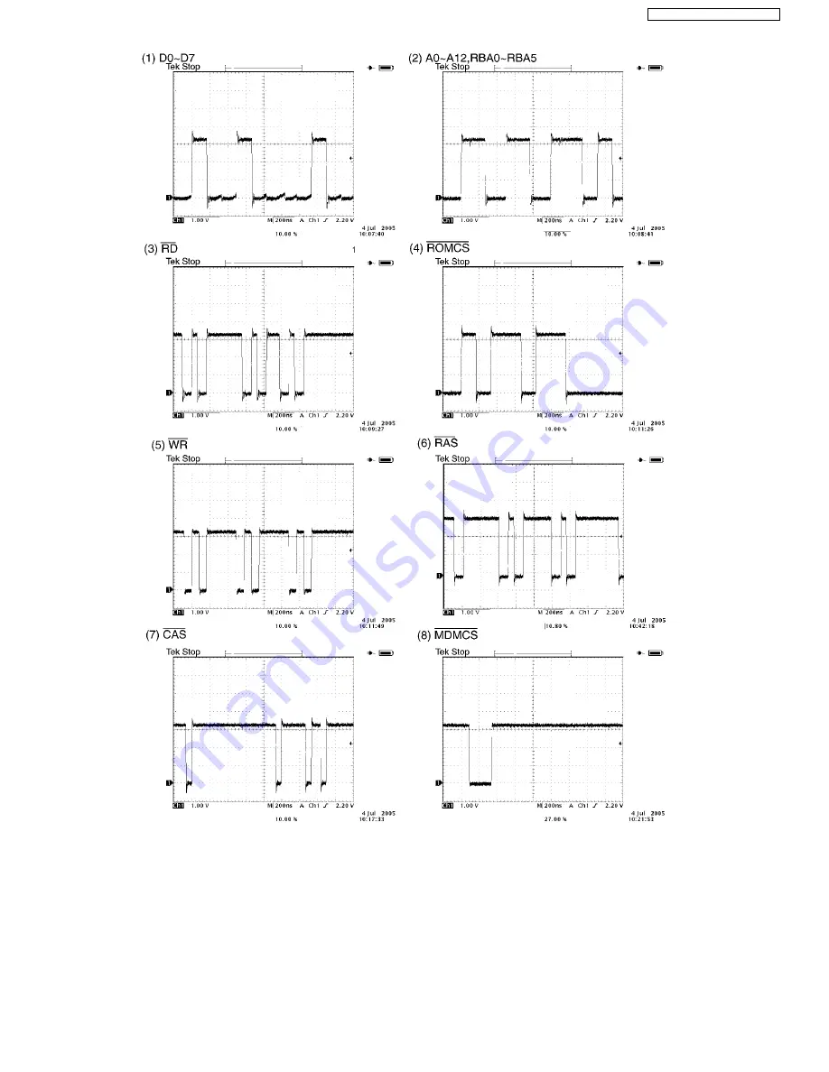
Normal Wave Patterns
Remarks:
When you use an oscilloscope to judge whether a signal to be tested is normal or NG, perform the signal check in exactly the
same order as in [List 1]. (If the ASIC fails to access the ROM, the ASIC cannot access DRAM normally.)
The digital circuit actually operates according to the timing combinations of these signals. If the timing of these signals is even
slightly delayed, the circuit will not work. Nor will it if the IC is defective and the output voltage level is not normal although the
timing of these signals is accurate enough to meet the specifications. (Make sure that your oscilloscope is calibrated before
starting a test.)
Therefore, it is imperative to confirm whether each IC outputs the signal at the correct level. (See the
I/O Pin No. Diagram
.) The
signal level should be constantly output at between 3.3V (H) and 0V (L) as described earlier.
Summary of Contents for KX-FT981LA-B
Page 11: ...11 KX FT981LA B KX FT987LA B 6 Technical Descriptions 6 1 Connection Diagram ...
Page 13: ...13 KX FT981LA B KX FT987LA B 6 2 1 General Block Diagram ...
Page 21: ...21 KX FT981LA B KX FT987LA B 6 4 2 Block Diagram ...
Page 23: ...23 KX FT981LA B KX FT987LA B ...
Page 63: ...63 KX FT981LA B KX FT987LA B 11 2 2 User Mode KX FT987 ...
Page 71: ...71 KX FT981LA B KX FT987LA B Countermeasure ...
Page 72: ...72 KX FT981LA B KX FT987LA B REFERENCE Test Mode P 54 ...
Page 73: ...73 KX FT981LA B KX FT987LA B REFERENCE Test Mode P 54 ...
Page 74: ...74 KX FT981LA B KX FT987LA B REFERENCE Test Mode P 54 ...
Page 75: ...75 KX FT981LA B KX FT987LA B REFERENCE Test Mode P 54 ...
Page 76: ...76 KX FT981LA B KX FT987LA B ...
Page 77: ...77 KX FT981LA B KX FT987LA B ...
Page 78: ...78 KX FT981LA B KX FT987LA B REFERENCE Test Mode P 54 ...
Page 82: ...82 KX FT981LA B KX FT987LA B ...
Page 108: ...108 KX FT981LA B KX FT987LA B NG Wave pattern Note Refer to NG Example P 113 ...
Page 110: ...110 KX FT981LA B KX FT987LA B I O and Pin No Diagram ...
Page 113: ...113 KX FT981LA B KX FT987LA B 12 5 6 2 NG Example ...
Page 115: ...115 KX FT981LA B KX FT987LA B ...
Page 120: ...120 KX FT981LA B KX FT987LA B 12 5 9 2 Troubleshooting Flow Chart ...
Page 126: ...126 KX FT981LA B KX FT987LA B 12 5 13 Thermal Head Section Refer to Thermal Head P 22 ...
Page 127: ...127 KX FT981LA B KX FT987LA B 13 Service Fixture Tools ...
Page 130: ...130 KX FT981LA B KX FT987LA B 14 1 2 How to Remove the Cutter Unit KX FT987 only ...
Page 131: ...131 KX FT981LA B KX FT987LA B 14 1 3 How to Remove the Lock Lever and Thermal Head ...
Page 133: ...133 KX FT981LA B KX FT987LA B 14 2 2 How to Remove the P C Boards and Power Cord ...
Page 136: ...136 KX FT981LA B KX FT987LA B 14 3 2 How to Remove the Operation Board LCD and Platen Roller ...
Page 137: ...137 KX FT981LA B KX FT987LA B 14 3 3 How to Remove the Separation Rubber Flap ...
Page 138: ...138 KX FT981LA B KX FT987LA B 14 4 Installation Position of the Lead Wires ...
Page 139: ...139 KX FT981LA B KX FT987LA B ...
Page 147: ...147 KX FT981LA B KX FT987LA B 15 2 3 4 Copying REFERENCE Sensor Section P 123 ...
Page 152: ...152 KX FT981LA B KX FT987LA B 16 1 4 Power Supply Board ...
Page 154: ...154 KX FT981LA B KX FT987LA B 16 3 Test Chart 16 3 1 ITU T No 1 Test Chart ...
Page 155: ...155 KX FT981LA B KX FT987LA B 16 3 2 ITU T No 2 Test Chart ...
Page 168: ...168 KX FT981LA B KX FT987LA B MEMO ...
Page 178: ...178 KX FT981LA B KX FT987LA B 20 1 1 Operation Panel Section KX FT981 ...
Page 179: ...179 KX FT981LA B KX FT987LA B 20 1 2 Operation Panel Section KX FT987 ...
Page 180: ...180 KX FT981LA B KX FT987LA B 20 1 3 Upper Cabinet Section ...
Page 181: ...181 KX FT981LA B KX FT987LA B 20 1 4 Lower Cabinet Section ...
Page 182: ...182 KX FT981LA B KX FT987LA B 20 1 5 Gear Block Section ...
Page 183: ...183 KX FT981LA B KX FT987LA B 20 1 6 Screws ...
Page 184: ...184 KX FT981LA B KX FT987LA B 20 1 7 Accessories and Packing Materials ...
Page 192: ...192 KX FT981LA B KX FT987LA B K N KXFT981LAB KXFT987LAB ...


