background image

INTRODUCTION

MCUK010801C8

Section 1

Issue 1

Service Manual

– 1 –

Revision 0

1

INTRODUCTION

INTRODUCTION

INTRODUCTION

INTRODUCTION

1.1.

Purpose of the Manual

This Service Manual contains the information and procedures required for installing, operating and servicing the Panasonic
GSM Personal Cellular Mobile Telephone system operating on GSM Digital Cellular Networks.

1.2.

Structure of the Manual

The manual is structured to provide service engineering personnel with the following information and procedures:
1.

General and technical information - provides a basic understanding of the equipment, kits and options, together with 
detailed information for each of the major component parts.

2.

Installation and operating information - provides instructions for unpacking, installing and operating the equipment.

3.

Servicing information - provides complete instructions for the testing, disassembly, repair and reassembly of each major 
component part. Step-by-step troubleshooting information is given to enable the isolation and identification of a 
malfunction, and thus determine what corrective action should be taken. The test information enables verification of the 
integrity of the equipment after any remedial action has been carried out.

4.

Illustrated parts list - provided to enable the identification of all equipment components, for the ordering of spare / 
replacement parts.

1.3.

Servicing Responsibilities

The  procedures  described  in  this  manual  must  be  performed  by  qualified  service  engineering  personnel,  at  an  authorised
service centre.
The service engineering personnel are responsible for fault diagnosis and repair of all equipment described in this manual.

WARNING

The equipment described in this manual contains polarised capacitors utilising liquid electrolyte. These devices are entirely safe provided 
that neither a short-circuit nor a reverse polarity connection is made across the capacitor terminals. FAILURE TO OBSERVE THIS 
WARNING COULD RESULT IN DAMAGE TO THE EQUIPMENT OR, AT WORST, POSSIBLE INJURY TO PERSONNEL RESULTING 
FROM ELECTRIC SHOCK OR THE AFFECTED CAPACITOR EXPLODING. EXTREME CARE MUST BE EXERCISED AT ALL TIMES 
WHEN HANDLING THESE DEVICES.

Caution

The equipment described in this manual contains electrostatic devices (ESDs). Damage can occur to these devices if the handling 
procedures described in Section 4 are not adhered to.

Caution

This equipment may contain an internal battery in addition to the external battery packs. These batteries are recyclable and should be 
disposed of in accordance with local legislation. They must not be incinerated, or disposed of as ordinary rubbish.

Summary of Contents for EB-GD95

Page 1: ...0 cc Weight 85 g Display Graphical chip on glass liquid crystal Alphanumeric 16 characters x 3 rows 2 lines of icons Illumination 4 LEDs for the LCD 8 LEDs for the keypad Green 1 LED Incoming call Green 1 Charging LED Red Keys 18 key Keypad Navigation key SIM Plug in type only External DC Supply Voltage 5 8 V Battery 3 7 V nominal 650mAh Li Ion Standby Time 150 hrs maximum Talk Time 270 minutes ma...

Page 2: ...the right to make changes to the specification or design without prior notice The information contained in this manual and all rights in any design disclosed therein are and remain the exclusive property of Matsushita Communication Industrial UK Ltd Other patents applying to material contained in this publication BULL CP8 PATENTS Comments or correspondence concerning this manual should be addresse...

Page 3: ...ed by PC Card 13 3 15 GSM Network Codes and Names 14 3 16 Glossary of Terms 18 4 DISASSEMBLY REASSEMBLY INSTRUCTIONS 4 1 General 19 4 2 Disassembly 19 4 3 Reassembly 23 5 TECHNICAL SPECIFICATIONS 5 1 Tx Characteristics 24 5 2 Rx Characteristics 25 6 TEST AND MEASUREMENT 6 1 Introduction 28 6 2 Any Layer Interstitial Via Hole ALIVH PCBs 28 6 3 External Testing 29 6 4 Complete Unit Setup 32 6 5 Chan...

Page 4: ...Issue 1 Section MCUK010801C8 Revision 0 iv Service Manual This page is left intentionally blank ...

Page 5: ... action has been carried out 4 Illustrated parts list provided to enable the identification of all equipment components for the ordering of spare replacement parts 1 3 Servicing Responsibilities The procedures described in this manual must be performed by qualified service engineering personnel at an authorised service centre The service engineering personnel are responsible for fault diagnosis an...

Page 6: ... Full Rate EFR speech codec 2 Dual Band E GSM 900 and GSM 1800 operation 3 Tegic T9 Text Entry 4 Voice Ringer 5 Desktop Handsfree function comprising integral echo cancellation and noise suppression 6 Wireless Application Protocol WAP Browser 7 E Mail access via Point to Point Protocol PPP 8 Backup Battery 9 Downloadable polyphonic melody ringtones 10 Clock Calculator and Currency Converter 11 Thr...

Page 7: ...ing charging Menu Icon Displays a small icon related to the current status of the telephone telephone is roaming on a non home network using the Call Divert feature or the telephone has Call Divert set shows that vibration alert is switched on shows that the telephone is in silent mode no tones flashes to indicate that there are unread text SMS messages Lit when SMS area is full indicates the tele...

Page 8: ... Personal Dial Key Provides instant access to one phone number Also provides shortcut to WAP Browser and to SMS Send Key Makes a call Clear Key Clears the last digit entered clears all digits when pressed and held or returns to the previous display End Key Ends a call or switches the telephone on off when pressed and held to Digit keys Enter wild numbers or pauses when pressed and held Where appro...

Page 9: ...the Phonebook Short Messages and Greeting Message areas Each time a key is pressed it will display the next character When another key is pressed or no key is pressed for a short time the cursor will move to the next position To cycle between Greek characters extended characters W numerals X and normal characters U press Key Character Operation T9 Normal Greek Extended Numeric Alternatives 0 P_ Pu...

Page 10: ...is SIM Network dependent Received List Send List Create User Defined Msg Review Parameters Broadcasts Receive Message List Topics Languages Auto Delete Lifetime Message Centre Report Protocol Messages Short Message E Mail Inbox Outbox Create Send Receive Review Parameters Clock Set Clock Format Alarm Set Power On Time Power Off Time Applications Games Voice Memo Download Melody Clock Function Calc...

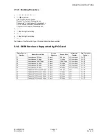
Page 11: ...urce 3 9 Public Man Machine Interface MMI 3 9 1 General It is possible to operate all GSM telephones in the same way using the Public MMI The following operations will work with all GSM telephones However this information is restricted to those operations supported by the telephone The and in the following procedures should be replaced by and respectively Also SND and END should be replaced with a...

Page 12: ...Enable SERVICE CODE SND Disable SERVICE CODE SND Temporary Suppress Identification 3 1 TELEPHONE NUMBER SND Temporary Display Identification 3 1 TELEPHONE NUMBER SND Service MMI Service Code All teleservices 10 Telephony 11 All data teleservices 12 Facsimile services 13 Short Message Services SMS 16 All teleservices except SMS 19 Voice group services 17 Service MMI Service Code All bearer services...

Page 13: ... TELECOM SERVICE TIME TO RING sec SND Clear SERVICE CODE TELECOMMUNICATION SERVICE SND Status SERVICE CODE TELECOMMUNICATION SERVICE SND Clear all Call Diverts 0 0 2 Call Ball Type Service Code All outgoing calls 33 Outgoing International calls 331 Outgoing International calls except those to the PLMN 332 All incoming calls 35 Incoming international calls when roaming 351 Set PASSWORD TELECOMMUNIC...

Page 14: ...y is deeply discharged it will take a short time before there is sufficient power in the telephone to light the battery level indicator Leave to charge for several minutes in temperatures between 5 C and 35 C Calls cannot be made The telephone is locked Unlock the telephone Menu Security Phone Lock Outgoing calls are barred Disable the outgoing call barring Menu Security Call Bar The telephone is ...

Page 15: ...ar Menu Messages Parameters Auto Delete Store Full PIN2 Invalidated The PIN2 is blocked permanently because the wrong PUK2 has been entered 10 times Services controlled by PIN2 cannot be used Contact the Service Provider Warning Store Full The message area is full New messages cannot be stored until some of the currently stored messages are deleted Continue Auto Redial List Full Redial list of uns...

Page 16: ...on is activated during manufacture and then enabled at a later stage Enabling disabling is available by entering a special key sequence immediately after power on Once the enable disable menu is shown it is possible to select the type of personalisation When personalisation is enabled it is only possible to disable it if the mobile contains an illegal SIM and the 16 digit Control Key CK is known F...

Page 17: ...ure Access Rate Information Transfer Error Correction Options 21 Asynchronous 300 bps Asynch 300 bps UDI or modem T or NT 22 Asynchronous 1 2 kbps Asynch 1 2 kbps UDI or modem T or NT 23 Asynchronous 1200 75 bps Asynch 1200 75 bps UDI or modem T or NT 24 Asynchronous 2 4 kbps Asynch 2 4 kbps UDI or modem T or NT 25 Asynchronous 4 8 kbps Asynch 4 8 kbps UDI or modem T or NT 26 Asynchronous 9 6 kbps...

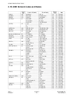
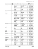
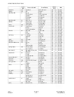
Page 18: ...o HR VIP 219 10 GSM 900 CYPRUS 357 CYTAGSM CY CYTAGSM 280 01 GSM 900 CZECH_REPUBLIC 42 EUROTEL GSM EUROTEL CZ 230 02 GSM 900 OSKAR OSKAR 230 03 not known Radio Mobil CZE PAEGAS CZ 230 01 GSM 900 DENMARK 45 SONOFON DK SONOFON 238 02 GSM 900 TDK MOBIL DK TDK MOBIL 238 01 GSM 900 Telia DK Telia DK 238 20 GSM 1800 mobilix mobilix 238 30 GSM 1800 EGYPT 20 EGY CLICK GSM EGY CLICK GSM 602 02 not known Mo...

Page 19: ...M 510 11 GSM 900 IND SATELINDOCEL IND SATELINDOCEL 510 01 GSM 900 TELKOMSEL IND TELKOMSEL 510 10 GSM 900 IRELAND 353 EIRCELL GSM IRL EIR GSM 272 01 GSM 900 IRL DIGIFONE IRL DIGIFONE 272 02 GSM 900 ITALY 39 BLU I BLU 222 98 GSM 1800 I WIND I WIND 222 88 GSM 1800 OMNITEL I OMNITEL 222 10 GSM 900 TELECOM ITALIA MOBIL I TIM 222 01 GSM 900 JORDAN 962 Fastlink Fastlink 416 01 GSM 900 KUWAIT 965 MTCNet K...

Page 20: ...Line BeeLine 250 99 GSM 1800 MTS MTS RUS 250 01 GSM 900 North West GSM North West GSM 250 02 GSM 900 SAUDI_ARABIA 966 EAE ALJAWWAL EAE ALJAWWAL 420 07 GSM 900 MoPTT DMTS 1 ALJAWWAL 420 01 GSM 900 SEYCHELLES 248 SEYCHELLES CELLULAR SERVICES CELLULAR SERVICE 633 01 GSM 900 SINGAPORE 65 M1 GSM M1 GSM SGP 525 03 GSM 900 ST GSM ST GSM SGP 525 01 GSM 900 ST GSM1800 SGP ST GSM1800 SGP 525 02 GSM 1800 SLO...

Page 21: ... TELSIM 286 02 GSM 900 PTT TURKCELL GSM TR TURKCELL 286 01 GSM 900 UKRAINE 380 GOLDEN TELECOM GOLDEN TELECOM 255 05 GSM 1800 UA KYIVSTAR UA KYIVSTAR 255 03 GSM 900 UA UMC UA UMC 255 01 GSM 900 UA WELLCOM UA WELLCOM 255 02 GSM 900 UNITED ARAB EMIRATES UAE 971 UAE ETISALAT ETISALAT G2 424 02 GSM 900 UNITED KINGDOM 44 BTCellnet UK BTCELLNET 234 10 GSM 900 ONE2ONE one2one 234 30 GSM 1800 ORANGE ORANGE...

Page 22: ...function Supplied by the service provider PIN Personal Identification Number used for SIM security Supplied by the service provider PIN2 Personal Identification Number used for the control of Fixed Dial Memory and call charge metering Supplied by the service provider PUK PUK2 PIN PIN2 Unblocking Key Used to unblock the PIN PIN2 Supplied by the service provider Registration The act of locking on to...

Page 23: ...skin contact device with a flexible cord which has an integral safety resistor of between 5k2 and 1M2 shall be used Containers All containers and storage must be of the conductive type 4 2 Disassembly 4 2 1 Case Removal 1 Remove the battery from the back of the telephone Remove the four case screws located inside the battery compartment Figure 4 1 Case Screw Removal WARNING The equipment described...

Page 24: ...g that the moulded hooks separate all the way up to point A Figure 4 2 Case Cover Separation 3 Repeat step 2 for the opposite side of the telephone Carefully twist the cover so that the hooks at position B and those at the corresponding position on the opposite side of the phone separate 4 Using a small screwdriver blade or similar blunt object depress one of the RF Shield lugs marked A and B in t...

Page 25: ...LCD assembly can now be removed from the PCB 3 To remove the LCD carefully lift the flexible PCB away from the two retaining lugs on the underside of the LCD Holder The flexible PCB can then be used to pull the LCD from the Holder Figure 4 5 Removing the LCD from its Holder 4 2 3 Case Mounted Components 1 Remove the keypad membrane by pressing on the navigation key until it can be peeled away from...

Page 26: ...he microphone holder Figure 4 7 Removal of Microphone 3 To remove the speaker first remove the retaining clip Then lift the speaker from the case by inserting a small screwdriver blade or similar blunt object underneath it Figure 4 8 Speaker Removal 4 To gain access to the DTHF speaker remove the RF Shield by depressing lug A or B and then lifting the shield away from the case Figure 4 9 RF Shield...

Page 27: ... may be removed from the RF shield by pushing on the underside of the motor body Figure 4 11 Removal of Vibrate Motor 6 Using a small screwdriver blade or similar blunt object depress the lug on the antenna base in order to release the entire antenna unit Figure 4 12 Antenna Removal 4 3 Reassembly Reassembly is the reverse of disassembly Ensure that the securing screws are not over tightened as th...

Page 28: ...tput RF Spectrum due to Modulation 5 1 4 Output RF Spectrum due to Switching Transients RMS Equal to or less than 5 Peak Equal to or less than 20 Offset from Centre Frequency kHz Maximum Level Relative to Carrier dB 100 0 5 200 30 250 33 400 60 600 to 1800 60 Offset from Centre Frequency kHz Maximum Level dBm E GSM 900 GSM 1800 400 19 22 600 21 24 1200 21 24 1800 24 27 Measurement conditions for o...

Page 29: ...GHz 0 to 10 MHz 100 kHz 300 kHz 30 30 1 0 1 710 GHz Excl relevant TX band 10 MHz 300 kHz 1 MHz 30 36 1 710 1 785 GHz P GSM 890 to 915 MHz 20 MHz 1 MHz 3 MHz 30 30 1 785 12 75 GHz DCS 1710 to 1785 MHz offset from edge of relevant TX band Relevant TX band 1 8 to 6 0 MHz 30 kHz 100 kHz 30 30 P GSM 890 to 915 MHz offset from DCS 1710 to 1785 MHz carrier Channels Propogation Conditions TUhigh Propogati...

Page 30: ... error rate Minimum No of samples TCH HS FER 4 598 13050 TCH HS class Ib BFI 0 0 404 148500 TCH HS class II BFI 0 7 725 25500 8500 20000 7600 20000 TCH HS UFR 6 250 9600 TCH HSL class Ib BFI or UFI 0 0 269 227000 Channels Propogation Conditions TUhigh Propogation Conditions RA Propogation Conditions HT Static Conditions Test Limit error rate Minimum No of samples Test Limit error rate Minimum No o...

Page 31: ...tics Frequency Small MS level in dBµVemf E GSM 900 GSM 1800 FR 600 kHz to FR 800 kHz 70 70 FR 800 kHz to FR 1 6 MHz 70 70 FR 1 6 MHz to FR 3 MHz 80 80 915 MHz to FR 3 MHz 90 FR 3 MHz to FR 980 MHz 90 FR 600 kHz to FR 800 kHz 87 1785 MHz to FR 3 MHz 87 835 MHz to 915 MHz 113 980 MHz to 1000 MHz 113 100 kHz to 835 MHz 90 1000 MHz to 12 75 GHz 90 100 kHz to 1705 MHz 113 1705 MHz to 1785 MHz 101 1920 ...

Page 32: ...a component is removed from the board Warping Property The ALIVH PCB has a smaller Young s Modulus and is therefore more pliant than conventional boards It is important that the ALVIH PCB is not bent when component placement is performed 6 2 2 Repair Procedures To prevent problems caused by moisture absorption it will be necessary to perform dehydration of ALIVH PCBs in a suitable oven or similar ...

Page 33: ...stment of the handheld unit can be performed with the outer case in place and the cradle connected For in depth fault finding the unit should first be disassembled as detailed in Section 4 and then the PCB Repair Jig used to connect the PCBs together externally as they would be found in normal use Fault tracing can then be performed on the PCBs using suitable test equipment such as spectrum analys...

Page 34: ...e Unit Under Test Power Supply Provides 12 V DC supply to Interface box IFB003 or IFB004 PCB Repair Jig Part No JT00067 This unit provides the necessary connections between the PCB Assembly and external test equipment Figure 6 2 PCB Repair Jig RF Adaptor Part No JT00068 This unit provides an RF connection between the unit under test and external test equipment Figure 6 3 RF Adaptor INTERFACE BOX M...

Page 35: ...lities Dummy Battery Part No JT00069 The dummy battery is used for battery calibration Figure 6 4 Dummy Battery Channel Box Software This is the test software for the telephone unit and should be installed onto the personal computer to be used for testing Case Separation Tool Part No JT00059 The Case Separation Tool is used to facilitate separation of the front cover and case Figure 6 5 Case Separ...

Page 36: ... the test equipment must be connected as shown The PCB Test Setup must be used to enable repair to PCBs Once repair replacement is complete the assembled unit must be tested and calibrated using the Complete Unit Test Setup 12V POWER SUPPLY INTERFACE BOX PC RS232 PCB REPAIR JIG GSM TESTER RF CABLE 12V POWER SUPPLY INTERFACE BOX PC RS232 GSM TESTER RF CABLE UNIT UNDER TEST RF ADAPTOR PCB TEST SETUP...

Page 37: ...held unit 1 Test Mode The Test Mode facility allows various sections of the handheld unit to be individually activated 2 Normal Mode The Normal Mode facility allows the handheld unit to be powered externally for call origination receiving operations NOTE A suitable test SIM card will be required which is compatible with the GSM test station 6 4 2 Power On into Test Mode 1 Connect the test equipmen...

Page 38: ...ds for further testing information 6 4 3 Power On in Normal Mode 1 Connect the test equipment as shown in Section 6 3 Figure 6 9 External Test Equipment Setup 2 Ensure that the following settings are made NOTE The Display will read GET STATION ADDRESS __ INFO __ a Interface Box IFB003 or IFB004 Power DOWN position IGN UP position MODE UP position b Power Supply IFB003 or IFB004 12V DC ON MODE UP p...

Page 39: ...he PC should resemble the one shown below Figure 6 11 PC Screen SCRN11 1 At the PC change the SOFT SIM field to read ENABLE Press ENTER 2 At the PC change the TEST MODE field to read TERM Press ENTER The UUT will power down and up again If the UUT is connected to a GSM test set after a delay of approximately five seconds the UUT will register service 3 To return to test mode set the SOFT SIM field...

Page 40: ...audio loop back from TX audio to RX audio without processing by the CODEC STOP PATH CONT Sets audio paths MOSO MIC off speaker off MESI MIC external speaker internal MESE MIC external speaker external MISI MIC internal speaker internal MISE MIC internal speaker external VOL BUZZ xx Sets buzzer volume between values 0 to 3 Min to Max VOL SIDE xx Sets 4 side tone volume levels between 0 dB and 18 dB...

Page 41: ...cedures are described in Section 7 4 Adjustment data selected during calibration is stored in Flash ROM 7 2 Ramping Gain The carrier power must be measured and calibrated for each power level at channel 62 7 2 1 E GSM 900 NOTE See Section 6 2 for a list of the equipment and setup procedures required to perform the following adjustment and calibration procedures Power Level PL Output Power dBm Chan...

Page 42: ...arget power then proceed to step 10 Power Level PL Output Power dBm Change dB Nominal Target Spec Min Max Min Max 0 29 05 28 8 29 3 28 8 29 3 3 1 27 8 27 3 28 3 27 0 28 8 3 5 2 26 25 5 26 5 25 27 4 3 24 23 5 24 5 23 25 4 5 4 22 21 5 22 5 21 23 4 5 5 20 19 5 20 5 19 21 4 5 6 18 17 5 18 5 17 19 4 7 16 15 5 16 5 15 17 4 8 14 13 5 14 5 13 15 4 9 12 11 5 12 5 11 13 4 10 10 9 5 10 5 9 11 4 11 8 7 5 8 5 ...

Page 43: ...t the Channel box press F7 to view the TRIM for the mid channel 8 Select VIEW TRIM PL MCH and make a note of this value 9 Perform the following calculation and make a note of the result New Trim Value Old TrimValue Required Power Measured Power x Change per dB step 5 table step 2 table ...

Page 44: ...CEDURES Issue 1 Section 7 MCUK010801C8 Revision 0 40 Service Manual 10 At the Channel box press F6 to program the TRIM for the mid channel 11 Select PROGRAM TRIM PL MCH GSM 12 Highlight the PL14 fieldand press ENTER ...

Page 45: ...in the following order 20 Save TRIM data 7 3 RSSI This procedure describes the calibration of RSSI on the mid channel This procedure must also be carried out for the low bottom channel and high top channel The procedure is as follows 1 Power the telephone into Test Set mode in the service channel box PL6 PL9 and PL19 Power levels between PL9 and PL6 Power levels between PL14 and PL9 Power levels b...

Page 46: ...GE CH and using the left right cursor keys select CH 70 Press ENTER 4 Highlight the SET AGC1 field and change the set value to 48 dB Press ENTER 5 Highlight the RSSI dBm field and press ENTER 6 If the measured power is not 90 1 then make the following calculation Record the result 7 At the channel box press F7 to view data and highlight TRIM OTHER RSSI offset value 90 MEASURED RSSI VALUE x 2 90 ME...

Page 47: ...Highlight RSSI Mch GSM and press ENTER 13 Make the following calculation RSSI Offset Value step 8 reading noted in step 6 Enter the result in to the RSSI Mch field 14 Press ENTER 15 Press ESC 16 Measure the RSSI level again by highlighting the RSSI dBm field again and press ENTER 17 Repeat steps 6 to 16 for both low bottom and high top channels Channel E GSM Frequency Bch E GSM 975 925 2 MHz Lch 1...

Page 48: ...trol Unit BCVCU is used to provide the necessary voltage levels for these checks The BCVCU replaces the two regulated power supplies and 82 Ohm resistor required to caibrate previous mobile products 1 Connect the telephone test battery BCVCU and Interface Box as shown in the diagram below Figure 7 1 Battery calibration test conections 2 Set the Interface box to POWER ON IGN and EXT PWR OFF 3 Set t...

Page 49: ...e Calibration 1 Enter Test Set mode in Service Channel Box 2 Press F4 and select VIEW ADC LINES 3 Observe the ADIN1 value This value is BAT VOLT HIGH If this reading is outside the range 564 664 then there is a fault and further investigation is required Otherwise record this value for later use ...

Page 50: ...89 there is a fault and further investigation is required Otherwise record this value for use later 7 Press N in the repeat yes no box then press ENTER 8 Press F6 Scroll down to and select TRIM OTHER 9 Scroll down to and select BAT VOLT HIGH Enter the value recorded in step 3 10 Press F6 Scroll down to TRIM OTHER and press ENTER 11 Highlight BAT VOLT LOW and press ENTER Type in the value recorded ...

Page 51: ...ES 4 Check the value for ADIN2 BAT TEMP If the value is outside the range 168 248 then there is a fault and further investigation is required Otherwise subtract this value from the theoretical value of 208 and record the result for later use 5 Press N in the repeat yes no box then press ENTER 6 Press F6 Scroll down and highlight TRIM OTHER Press ENTER 7 Highlight BAT TEMP and press ENTER to select...

Page 52: ...ER 3 Holding down the Shift key press F4 Select PROG CHARG DAC DATA 4 Enter a value of 442 5 Disconnect VBAT by setting the BCVCU Voltage switch to OFF 6 Measure the voltage across the Test Battery terminals If the voltage is within the range 4 2 V 5 mV proceed to step 11 Otherwise calculate the difference DAC STEP as follows difference measured voltage 4 2 V 7 4 mV ...

Page 53: ...e for use later 11 Press F6 Highlight TRIM OTHER and press ENTER Highlight DAC REFERENCE and press ENTER 12 Enter the value recorded in step 10 7 4 5 Current Charging ADC Calibration It is important to monitor the current when charging the Li ion battery both to protect against over current and to determine when charging is complete The telephone uses the VCC3 and MADC ICHG connections of NAUSICA ...

Page 54: ...nvestigation is required Otherwise calculate the difference between the recorded value and the theoretical value of 161 Record this value for use later 3 Press F6 and select TRIM OTHER Select COMP OFFSET and enter the value recorded in step 2 4 Press F9 Wait for the prompt Saving EV Trim data to disappear turn OFF the power supplies and disconnect the telephone ...

Page 55: ...09 6RA507AADA RF CAP SILVER M109 6RA507 RF CAP BLACK M110 2FA564A SHIELD CASE GD95 M111 6HA779A SPEAKER CUSHION M112 4HA532A ANTENNA CONTACT M114 4CA531AAAA H S JACK CAP SILVER M114 4CA531AABA H S JACK CAP BLACK M115 2RA648A RECEIVER HOLDER M116 3Z70054B SCREW CASE COVER M117 3Z70054B SCREW CASE COVER M118 3Z70054B SCREW CASE COVER M119 3Z70054B SCREW CASE COVER Ref Part Number Description 001 HH7...

Page 56: ...ECTOR I O 14 WAY SMD 009 JC76001A AUDIO JACK SOCKET 2 5mm 012 ML616S BUTTON CELL 3V 013 K3ZZ00200009 HOLDER FOR BATTERY CELL 014 015 PY76041A CONNECTOR BATTERY 2 PIN SMD 016 PY76079A CONNECTOR BATTERY 3 PIN SMD 017 PY76078A CONNECTOR LCD 14 PIN 018 JS76006A CONNECTOR SIM GD95 M104 2QA618A LCD BACKLIGHT GD95 002 014 M104 017 007 012 013 016 C 018 009 008 015 004 10459 1 Ref No Part No Part Name Des...

Page 57: ...50V X7R C2 C311 F1G1H102A457 CAP CER 1nF 10 50V X7R B1 C312 F1H0J1050009 CAP CER 1uF 10 6 3V X5R B1 C313 ECJ1VB1H222K CAP CER 2 2nF 10 50V X7R B1 C314 F1G1E221A046 CAP CER 220pF 5 25V NPO B1 C316 F1G1H101A422 CAP CER 100pF 5 50V NP0 B1 C317 F1G1C1030001 CAP CER 10nF 10 16V X7R B1 C318 F1G1H101A422 CAP CER 100pF 5 50V NP0 B1 C319 F1G1H101A422 CAP CER 100pF 5 50V NP0 B1 C321 ECJ0EC1H330J CAP CER 33p...

Page 58: ...001 DIODE HVC350BTRF VARICAP 16V S B1 D302 B0CCAB000001 DIODE HVC350BTRF VARICAP 16V S B1 D601 MAZS0470GL DIODE MAZS0470G ZENER 4 7V F4 Ref No Part No Part Name Description Grid D602 MAZS0470GL DIODE MAZS0470G ZENER 4 7V F4 D603 MAZS0470GL DIODE MAZS0470G ZENER 4 7V F1 D604 B0BD6R800004 DIODE UMZ6 8EN ZENER 6 8V QUAD F2 D605 B0JCMC000004 DIODE RB491DT146 SCHOTTKY 20V C2 D606 B0JCDC000001 DIODE RB5...

Page 59: ...R835 ERJ2GEJ271X RES 270 OHM 5 1 16W D4 R836 ERJ2GEJ271X RES 270 OHM 5 1 16W D4 R837 ERJ2GEJ271X RES 270 OHM 5 1 16W D4 R838 ERJ2GEJ271X RES 270 OHM 5 1 16W D4 R839 ERJ2GEJ271X RES 270 OHM 5 1 16W D4 R840 ERJ2GEJ271X RES 270 OHM 5 1 16W D4 R842 ERJ2GEJ271X RES 270 OHM 5 1 16W D4 R844 EXB24V151JX RES NETWORK 150 OHMx2 5 R845 EXB24V221JX RES NETWORK 220 OHMx2 5 R846 ERJ2GEJ4R7X RES 4 7 OHM 5 1 16W D...

Page 60: ...95DPK07 SLOVAK GD95DPK08 FRENCH GD95DPK09 GERMAN EU WARRANTY GD95DPK10 ENGLISH PUK GD95DPK11 ENGLISH EU WARRANTY GD95DPK12 ENGLISH GD95DPK13 FINNISH EU WARRANTY GD95DPK15 FRENCH EU WARRANTY GD95DPK16 GERMAN EU WARRANTY GD95DPK17 GREEK EU WARRANTY GD95DPK18 HUNGARIAN GD95DPK19 ITALIAN EU WARRANTY GD95DPK20 NORWEGIAN EU WARRANTY GD95DPK21 POLISH GD95DPK22 PORTUGUESE EU WARRANTY GD95DPK23 RUSSIAN GD9...

Page 61: ...CIRCUIT DIAGRAMS MCUK010801C8 Section 9 Issue 1 Service Manual 57 Revision 0 9 CIRCUIT DIAGRAMS Figure 9 1 GD95 Circuit Diagram Logic A4 A4 EB GD95 EB GD95C ...

Page 62: ...CIRCUIT DIAGRAMS Issue 1 Section 9 MCUK010801C8 Revision 0 58 Service Manual Figure 9 2 GD95 Circuit Diagram RF A4 A4 EB GD95 EBGD95C ...

Page 63: ...LAYOUT DIAGRAMS MCUK010801C8 Section 9 Issue 1 Service Manual 59 Revision 0 10 LAYOUT DIAGRAMS Figure 10 1 PCB Layout Diagram 1 2 A B C D F E ...

Page 64: ...LAYOUT DIAGRAMS MCUK010801C8 Section 9 Issue 1 Service Manual 60 Revision 0 D C E A B F 3 4 ...

Page 65: ...MCUK010801C8 Section 9 Service Manual 57 9 CIRCUIT DIAGRAMS Figure 9 1 GD95 C A4 A4 EB GD95 EB GD95C ...

Page 66: ...CIRCUIT DIAGRAMS on 9 Issue 1 Revision 0 GD95 Circuit Diagram Logic A4 A4 ...

Page 67: ...CIRCUIT DIAGRAMS Issue 1 Section 9 Revision 0 58 Figure 9 2 GD95 Cir A4 A4 ...

Page 68: ...9 MCUK010801C8 Service Manual GD95 Circuit Diagram RF A4 A4 EB GD95 EBGD95C ...

Reviews: