Electrical Adjustment for AJ-BS900HEN & CA900HEN
ELE-15
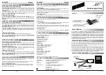
7. BS DIGITAL
7-1. Carrier Balance Adjustment
BOARD
BS DIGITAL
TP
ENC1 OUT
ADJ.
VR21 [BAL2], VR22 [B-Y BLK BAL]
VR18 [BAL1], VR19 [R-Y BLK BAL]
INPUT
AJ-BS900H Internal Color bar signal : ON
M. EQ
Vector scope (with 75
Ω
termination), 5x mode
SPEC.
As shown below
1. Connect Vector scope to ENC OUT1 and then
adjust VR21 so that the two vector dots are in
parallel with V axis on the scope.
2. Adjust VR22 so that the two vector dots meet to V
axis on the scope.
3. Adjust VR18 so that the two vector dots become
equal distance (A = B) from center position on V
axis of the scope.
4. Adjust VR19 so that the two vector dots come to
center position of the scope.
A
B
A
B
A
B
Summary of Contents for DVCPRO AJ-CA901P
Page 3: ...3 AJ CA901MC...
Page 4: ...4 AJ BS901P EN...
Page 5: ...5...
Page 6: ...6 AJ BS901MC...
Page 7: ...7...
Page 9: ...9...
Page 10: ...10...
Page 11: ...11...
Page 12: ...12...
Page 13: ...FCD0310NTKE448E449...
Page 20: ...BLOCK DIAGRAM CONTENTS BS AUDIO BLOCK DIAGRAM BLK 1...
Page 103: ...3 AJ CA900EN AJ CA900HEN...
Page 104: ...4 AJ BS900P AJ BS900HP...
Page 105: ...5...
Page 106: ...6 AJ BS900EN AJ BS900HEN...
Page 107: ...7...
Page 108: ...8 AJ RP900P EN AJ YA901P EN AJ YA600P...
Page 110: ...10 P ONLY...
Page 111: ...11 EN ONLY...
Page 112: ...12 EN ONLY...
Page 113: ...FCD0201KAOE286 E287 E289 E335 E392...
Page 127: ...6 CIRCUIT BOARD LAYOUT INF 13 HP EN...
Page 153: ...BS FRONT BLOCK DIAGRAM BLK 7 P2 2 P2 1 P2 4 P2 5 P1 7 P1 8 P1 5 P1 1 2 3 4 For RCOP unit...
Page 154: ...BS POWER BLOCK DIAGRAM BLK 8...
Page 155: ...POWER PROTECT BLOCK DIAGRAM BLK 9...
Page 215: ...CAM MOTHER C B A VEP20816 CBA 1 FOIL SIDE COMPONENT SIDE...
Page 227: ...BS POWER C B A VEP21248 CBA 13 FOIL SIDE REF LOC IC1 C1 IC2 C3 IC25 A3 IC26 A2 VR1 D4...
Page 231: ...BS SDI C B A VEP23517 CBA 17 FOIL SIDE REF LOC IC6 A4 IC7 A4 IC26 B8 Q3 B8...