5 . 2 . 3 . 7
Sensor
output adjustment
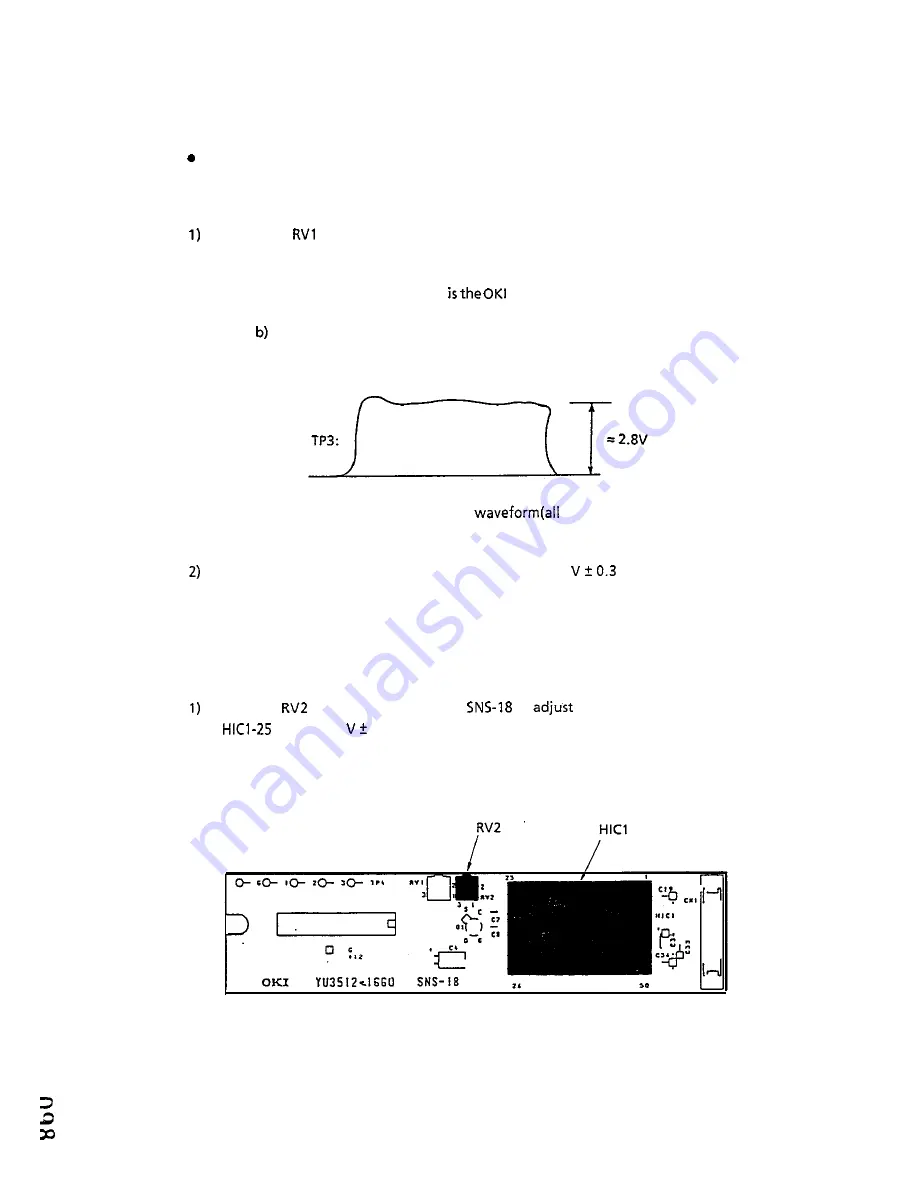
White signal output adjustment
Procedures:
Adjust the
potentiometer for a test-point TP3 output level of 2.8 V as a white
signal.
Note :
a)
The document to be used
test chart.
Make this adjustment after the fluorescent lamp has been continuously
lit for at least 10 minutes (for lighting stabilization).
Fig. 5.2.22
Sensor output
white signal)
Verify that the test-point TP4 output level is 2.8
V, using the above
document.
5.2.3.8
Black slice-level adjustment
Procedure:
Use the
potentiometer on the
to
the output voltage at the
pin as 1.47
0.03 V range.
* Do the above procedure at NORMAL mode of Type of Original.
Fig. 5.2.23
Black slice-level adjustment point
5 - 2 3
Summary of Contents for OKIFAX OF-38
Page 1: ...OfClFAx OF 38 Facsimile Transceiver HELD SERVICE HANDBOOK...
Page 2: ...OKIFAX OF 38 FACSIMILE TRANSCEIVER FIELD SERVICE HANDBOOK 0 0...
Page 7: ...C H A P T E R I GENERAL INFORMATION 0 0 s...
Page 8: ...CHAPTER 1 GENERAL INFORMATION 1 1 Features l l 1 2 GeneralAppearance l 3 0 0 c7...
Page 12: ...Fig 1 2 3 Operation Control Panel of the OKIFAX OF 38 l 4...
Page 13: ...0 0 co CHAPTER 2 SPECIFICATIONS...
Page 31: ...2 1 8...
Page 39: ...2 2 6...
Page 52: ...09s r El 1 SLl r pr Fig 2 1 General appearance and dimensionsof the OKIFAX OF 38 2 39...
Page 53: ...CHAPTER 3 lNSTALi_ATION...
Page 77: ...Table3 7 3 PTT parameter 3 2 3...
Page 112: ...Fig 3 13 1 Flow chart for typical message reception 3 5 8...
Page 113: ...Fig 3 13 2 Flow chart for typical message transmission 3 59...
Page 114: ...CHAPTER 4 MAINTENANCE...
Page 122: ...4 7...
Page 134: ...4 19...
Page 140: ......
Page 141: ......
Page 142: ...VW...
Page 143: ...4 28...
Page 144: ...P...
Page 145: ...4 30...
Page 146: ...1z N 4 31...
Page 147: ...l 4 32...
Page 148: ...4 33...
Page 149: ...4 34...
Page 150: ...4 35...
Page 151: ......
Page 152: ...4 37...
Page 153: ......
Page 154: ...4 39...
Page 155: ...4 40...
Page 156: ...4 41...
Page 157: ...4 42...
Page 158: ...4 43...
Page 159: ...4 44...
Page 160: ...CHAPTER 5 ADJUSTMENT...
Page 174: ...n mmmmm m mrm m 5 1 3...
Page 175: ...3 Scanner assembly SNS 18 PC BOARD SCREW SHIELDING PLATE Fig 5 2 4 Scanner assembly 5 14...
Page 186: ...CHAPTER 6 TROUSLESHOOTING...
Page 191: ...0 0 0 Fig 6 1 1 MODEM PC board 6 4...
Page 198: ...Li YU3512 1667 Fig 6 1 2 NCU 181 PC board JC3 6 1 1...
Page 211: ...Note No INo 6 2 4...
Page 214: ...6 2 4 Document Skew Put a smaller original in the carrier sheet and fed them together 6 2 7...
Page 220: ...C H A P T E R 7 DISASSEMBLY ASSEMBLY P...
Page 225: ...f 3z _ d 7 4...
Page 252: ...5 Remove a screw 0 SCREW 6 Remove the two screws Fig 7 3 11 3 SCREWS BOARD Fig 7 3 11 4 7 31...
Page 268: ...CHAPTER 8 BRIEF TECHNICAL DESCRIPTION...
Page 270: ...OKIFAX OF 38 overall circuit diagram Fig 8 1 1 m _ n 111 I I 1 Cl...
Page 271: ...t j_1 I 1 I I 1 c I_ c 8 3...
Page 273: ...m I j jj Read hugeData _ _t PrintlmageData...
Page 274: ...1 I _ __ __ _ M B 1 Fig 8 2 2 _ OKIFAX OF 38 G3 data send signal flow...
Page 275: ......
Page 276: ......
Page 277: ......
Page 278: ......
Page 280: ...I a 12...
Page 283: ...r 1 A J a 15...
Page 284: ......


