


Symphony SoundBite Demo User’s Guide
6
Freescale
Semiconductor
2.2
Running the Demonstration Application
When power is applied to the Symphony SoundBite board, the status LED (LED13) will light. The reset manager (U11) de-
asserts the reset line of the DSP (U1) after a period of time, causing the DSP to read the boot mode switches (SW2 positions
4:1). As configured in Table 2-1, the boot mode switches select Boot Mode 9 (boot from serial I
2
C EEPROM). SW2 switch
positions 6:5 connect the SDA and SCL lines of the I
2
C EEPROM (U6) to the DSP (U1). The DSP downloads the
application code from EEPROM to internal RAM and then executes it. Depressing the RESET switch (SW3) is equivalent
to power-cycling the board.
When the demonstration application starts up, it configures the DSP’s GPIO pins such that the DIP switches may be read
and the general purpose LEDs may be toggled on and off. The status of the DIP switch is then read to determine the
behavior (as described in Table 2-2) that the user desires, and the AK4584 (U5) is configured accordingly. Next, interrupts
are enabled, which allows the audio signals to be processed by the DSP. In the main loop of the application, an LED
(LED9) flashes a heart beat to indicate that the DSP is up and running. The DIP switch status is continually read, with the
state of each switch constantly displayed at LED1 through LED8.
To run a different configuration of the demonstration application, change SW1 to the desired setting (according to Table 2-
2) and reset the board using the RESET switch (SW3) (or power-cycle the Symphony SoundBite board).
For more about the internal workings of the demonstration application, refer to the application source code and the
Symphony SoundBite Assembly Project Template document.
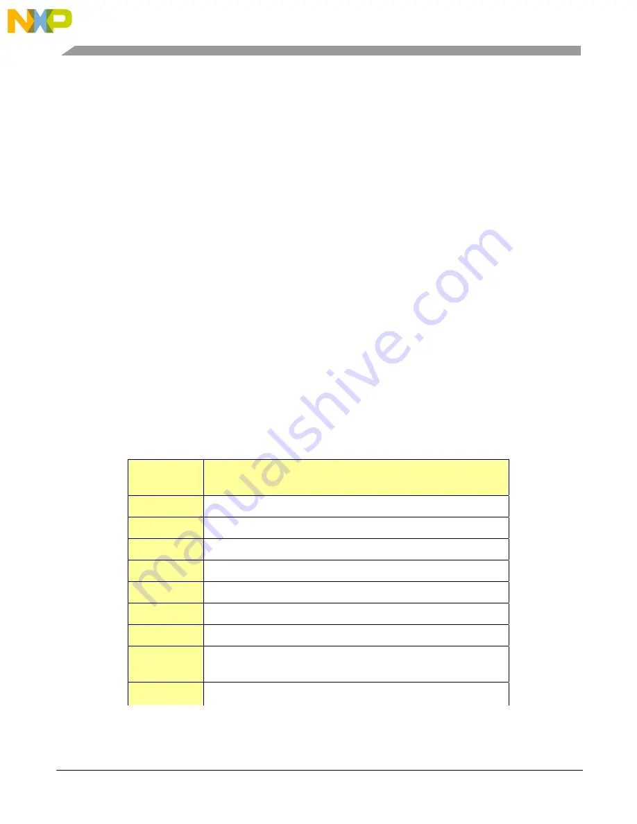
Table 2-2: Configurations for SW1 DIP Switch
SW1
1234 5678
Demonstration Application Configuration
1000 0000
J1 optical input passes through to all outputs.
0100 0000
J3 analog input passes through to all outputs.
0010 0000
J5 analog input passes through to all outputs.
0001 0000
J7 analog input passes through to all outputs.
0000 1000
Individual channel pass-through: J1>J2, J3>J4 , J5>J6, J7>J8.
0000 0100
Generates 1 kHz on all outputs
0000 0010
Generates sine waves of various frequencies.
0000 0001
Generates sine waves of various frequencies (different from above).
1111 1111
J7 analog input > J2 optical output
J1
i
l i
J4 J6 J8