


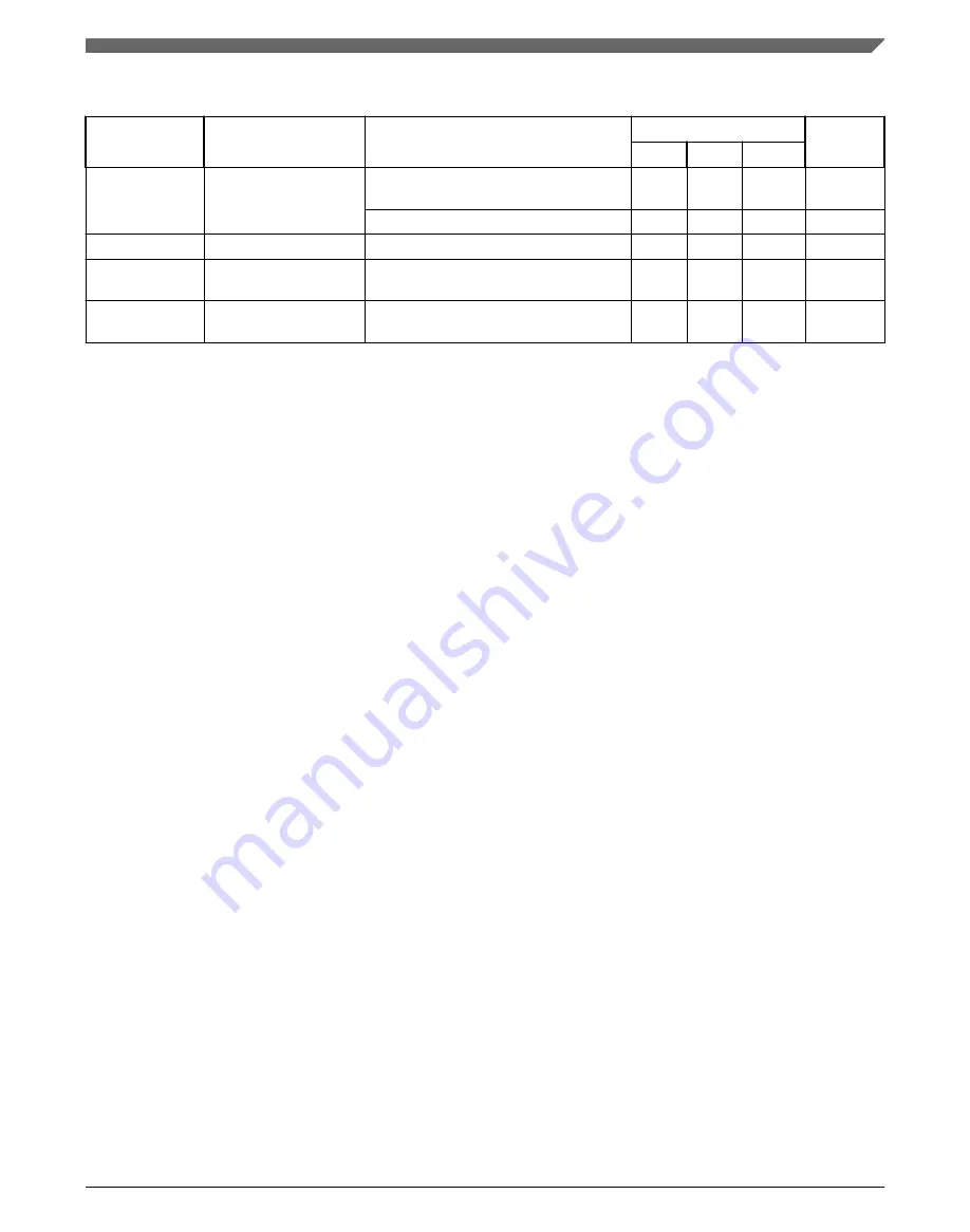
Table 20. SDn ADC electrical specification (continued)
Symbol
Parameter
Conditions
Value
Unit
Min
Typ
Max
C
S_D
S/D ADC sampling
capacitance after
sampling switch
GAIN = 1, 2, 4, 8
—
—
75*GAI
N
fF
GAIN = 16
—
—
600
fF
I
BIAS
Bias consumption
At least 1 ADCD enabled
—
—
3.5
mA
I
ADV_D
ADCD supply
consumption
ADCD enabled
—
2.5
8
mA
Σ
I
ADR_D
Reference current for
one SDADC
ADCD enabled
—
10
50
µA
1. For input voltage above the maximum and below the clamp voltage of the input pad, there is no latch-up concern, and the
signal will only be 'clipped'.
2. VINP is the input voltage applied to the positive terminal of the SD ADC.
3. VINM is the input voltage applied to the negative terminal of the SD ADC.
4. For Gain=16, SDADC Resolution is 15 bit.
5. Offset and gain error due to temperature drift can occur in either direction (+/-) for each of the SDADCs on the device.
6. Calibration of gain is possible when gain = 1. Offset Calibration should be done with respect to 0.5*V
DD_HV_ADR_SD
for
differential "differential mode" and single ended mode with negative input=0.5*V
DD_HV_ADR_SD
". Offset Calibration should
be done with respect to 0 for "single ended mode with negative input=0". Both Offset and Gain Calibration is guaranteed
for +/-5% variation of V
DD_HV_ADR_SD
, +/-10% variation of V
DD_HV_ADV_SD
, +/-50 C temperature variation.
7. S/D ADC is functional in the range 3.6V < V
DD_HV_ADV_SD
< 4.5V and 3.0V < V
DD_HV_ADR_SD
< 4.5 V, SNR paramter
degrades by 9 dB.
8. Input impedance in differential mode Z
IN
= Z
DIFF
9. Input impedance given at f
ADCD_M
= 16 MHz. Impedance is inversely proportional to SDADC clock frequency. Z
DIFF
(f
ADCD_M
) = (16 MHz / f
ADCD_M
) * Z
DIFF
, Z
CM
(f
ADCD_M
) = (16 MHz / f
ADCD_M
) * Z
CM
.
10. Input impedance in single-ended mode Z
IN
= (2 * Z
DIFF
* Z
CM
) / (Z
DIFF
+ Z
CM
)
11. V
INTCM
is the Common Mode input reference voltage for the SDADC. It has a nominal value of (V
RH_SD
- V
RL_SD
) / 2.
12. The ±1% passband ripple specification is equivalent to 20 * log10 (0.99) = 0.873 dB.
13. Propagation of the information from the pin to the register CDR[CDATA] and flags SFR[DFEF], SFR[DFFF] is given by the
different modules that need to be crossed: delta/sigma filters, high pass filter, fifo module, clock domain synchronizers.
The time elapsed between data availability at pin and internal S/D module registers is given by the following formula:
REGISTER LATENCY = tL 0.5/f 2 (~+1)/f 2(~+1)fPBRIDGEx_CLK where fADCD_S is
the frequency of the sampling clock, fADCD_M is the frequency of the modulator, and fPBRIDGEx_CLK is the frequency
of the peripheral bridge clock feeds to the ADC S/D module. The (~+1) symbol refers to the number of clock cycles
uncertainty (from 0 to 1 clock cycle) to be added due to resynchronization of the signal during clock domain crossing.
Some further latency may be added by the target module (core, DMA, interrupt) controller to process the data received
from the ADC S/D module.
14. This capacitance does not include pin capacitance, that can be considered together with external capacitance, before
sampling switch.
12 Temperature sensor
The following table describes the temperature sensor electrical characteristics.
Temperature sensor
SPC5746R Microcontroller Data Sheet, Rev. 6, 06/2017
NXP Semiconductors
39


