NHM–7
System Module LA5
PAMS Technical Documentation
B–13
Issue 1 10/2001
Nokia Corporation
GSM RF – BB Interface
(Version 1.3 Edit 35) for layout version 17
Page 1: ...Technical Documentation Programs After Market Services PAMS Copyright 2001 Nokia Corporation All Rights Reserved NMP Part No 0275518 NHM 7 SERIES CELLULAR PHONES NHM 7 issue 1 10 2001 ...
Page 2: ...NHM 7 Foreword PAMS Technical Documentation Issue 1 10 2001 Page 2 Nokia Corporation AMENDMENT RECORD SHEET Amendment Date Inserted By Comments 10 2001 J Rantala Issue 1 ...
Page 3: ...IES CELLULAR PHONES SERVICE MANUAL CONTENTS 1 Foreword 2 General Information 3 System UI Module LA5 LK5 4 Part lists 5 Product Variants NHM 7 6 Service Software Concepts 7 Service Tools 8 Disassembly Instructions 9 Troubleshooting Instructions 10 Non serviceable Accessories 11 Schematic Diagrams ...
Page 4: ...s will be included with service bulletins While every endeavour has been made to ensure the accuracy of this document some errors may exist If any errors are found by the reader NOKIA Corporation should be notified in writing Please state Title of the Document Issue Number Date of publication Latest Amendment Number if applicable Page s and or Figure s in error Please send to Nokia Corporation NMP...
Page 5: ...LLY EXPLOSIVE ATMOSPHERES EG PETROL STATIONS SERVICE STATIONS BLASTING AREAS ETC 3 OPERATION OF ANY RADIO TRANSMITTING EQUIPMENT INCLUDING CELLULAR TELEPHONES MAY INTERFERE WITH THE FUNCTIONALITY OF INADEQUATELY PROTECTED MEDICAL DEVICES CONSULT A PHYSICIAN OR THE MANUFACTURER OF THE MEDICAL DEVICE IF YOU HAVE ANY QUESTIONS OTHER ELECTRONIC EQUIPMENT MAY ALSO BE SUBJECT TO INTERFERENCE Cautions 1 ...
Page 6: ...NHM 7 Foreword PAMS Technical Documentation Issue 1 10 2001 Page 6 Nokia Corporation This page intentionally left blank ...
Page 7: ...PAMS Technical Documentation NHM 7 Series Transceivers Issue 1 10 2001 Nokia Corporation General Information ...
Page 8: ...ral Information PAMS Technical Documentation Page 2 Issue 1 10 2001 Nokia Corporation CONTENTS The Product 3 Handportable 3 Desktop Option 4 Product and Module List 5 General Specifications of Transceiver NHM 7 6 ...
Page 9: ...card below the back cover of the phone Back mounted antenna no connection for external antenna Jack style UI with two soft keys Handportable 1 3 4 5 6 ACP 7E ACP 7C ACP 7X ACP 7H ACP 7A ACP 7U NHM 7 2 HDD 1 Item Name Type code Material code 1 Transceiver See Product Variants Standard battery Li ion BLB 2 0271570 2 Headset HDD 1 0273302 3 Standard Charger Euro plug 207 253 Vac ACP 7E 0675144 4 Stan...
Page 10: ... 8K ACP 8X ACP 8U ACP 8C ACP 8A DCD 1 1 NHM 7 Item Name Type code Material code 1 Transceiver See Product Variants 2 Desk Stand DCD 1 0272865 3 Travel Charger Euro plug 90 264 Vac ACP 8E 0272169 Travel Charger Korea plug 90 264 Vac ACP 8K 0273111 4 Travel Charger UK plug 90 264 Vac ACP 8X 0272172 5 Travel Charger US plug 90 264 Vac ACP 8U 0675196 Travel Charger China plug 90 264 Vac ACP 8C 0675211...
Page 11: ...tandard Charger AUS 216 264 Vac 0675148 ACP 8E Travel Charger EUR 90 264 Vac 0272169 ACP 8K Travel Charger Korea 90 264 Vac 0273111 ACP 8X Travel Charger UK 90 264 Vac 0272172 ACP 8U Travel Charger US 90 264 Vac 0675196 ACP 8C Travel Charger China 90 264 Vac 0675211 ACP 8A Travel Charger Australia 90 264 Vac 0271637 LCH 9 Mobile Charger 0675120 PPH 1 Plug in HF Car Kit 0272170 MBD 10 Mobile Holder...
Page 12: ...y band EGSM 880 890 MHz GSM900 890 915 MHz GSM1800 1710 1785 MHz Output power GSM900 5 33 dBm 3 2 mW 2 W GSM1800 0 30 dBm 1 0 mW 1 W Duplex spacing GSM900 45 MHz GSM1800 95 MHz Number of RF channels EGSM 50 GSM900 124 GSM1800 374 Channel spacing 200 kHz Number of TX power levels GSM900 15 GSM1800 16 Sensitivity static channel GSM900 102 dBm GSM1800 102 dBm norm cond only Frequency error static cha...
Page 13: ...PAMS Technical Documentation NHM 7 Series Transceivers Issue 1 10 2001 Nokia Corporation System Module UI ...
Page 14: ... Internal speaker 12 AC and DC Characteristics of RF BB voltage supplies 13 AC and DC Characteristics of RF BB digital signals 14 AC and DC Characteristics of RF BB analogue signals 15 External Signals and Connections 16 UI board to board connector 16 LCD connector 17 DC connector 18 Headset connector 18 SIM connector 19 Functional Description 20 Modes of Operation 20 Supply Voltage Regulation 21 ...
Page 15: ...Edit 156 for layout version 15 A 4 Audio Interface Version 1 3 Edit 15 for layout version 15 A 5 UEM of BB Version 2 0 Edit 164 for layout version 15 A 6 Light Filtering Version 2 0 Edit 34 for layout version 15 A 7 Display and Keyboard Interface Version 1 3 Edit 201 for layout version 15 A 8 Infrared Module Version 2 0 Edit 37 for layout version 15 A 9 FM Radio Version 1 3 Edit 104 for layout ver...
Page 16: ...iltering Version 2 0 Edit 34 for layout version 17 B 7 Display and Keyboard Interface Version 1 3 Edit 210 for layout version 17 B 8 Infrared Module Version 2 0 Edit 38 for layout version 17 B 9 FM Radio Version 1 3 Edit 110 for layout version 17 B 10 SIM Reader Version 1 3 Edit 48 for layout version 17 B 11 UPP and decoupling capacitors Version 2 0 Edit 91 for layout version 17B 12 GSM RF BB Inte...
Page 17: ...NHM 7 System Module UI PAMS Technical Documentation Page 5 Issue 1 10 2001 Nokia Corporation This page intentionally left blank ...
Page 18: ...lf rate speech decod ing An integrated IR link provides a connection between two NHM 7 trans ceivers or a transceiver and a PC internal data or a transceiver and a printer The small SIM Subscriber Identity Module card is located under the battery SIM interface supports both 1 8V and 3V SIM cards Electrical Modules The radio module consists of Radio Frequency RF and baseband BB User Interface UI co...
Page 19: ...only the circuits needed for power up are supplied In the active mode all the circuits are supplied with power although some parts might be in the idle state part of the time The charge mode is effective in parallel with all previous modes The charge mode itself consists of two different states i e the fast charge and the maintenance mode The local and test modes are used for alignment and testing...
Page 20: ...wire type of Nokia chargers Three wire chargers are treated like two wire ones There is not separate PWM output for controlling charger but it is connected to GND inside the bottom connector Charging is controlled by UEM ASIC Universal Energy Man agement and EM SW running in the UPP Universal Phone Processor BLB 2 Li ion battery is used as main power source for the phone Block Diagram UEM UI SIM U...
Page 21: ...DSP digital control Data transmission between the UEM and the UPP is implemented using two serial busses DBUS for DSP and CBUS for MCU RF ASIC Hagar is controlled through UPP RFBUS serial interface There is also separate signals for PDM coded audio Digital speech processing is handled by the DSP in side UPP ASIC UEM is a dual voltage circuit the digital parts are running from the baseband supply 1...
Page 22: ...ASH2 2 70V 2 78V 2 86V Imax 40mA VSIM 1 745V 2 91V 1 8V 3 0V 1 855V 3 09V Imax 25mA ISleep 0 5mA VIO 1 72V 1 8V 1 88V Imax 150mA ISleep 0 5mA VCORE 1 0V 1 235V 1 425V 1 710V 1 053V 1 3V 1 5V 1 8V 1 106V 1 365V 1 575V 1 890V Imax 200mA ISleep 0 2mA Default value 1 5V RF Regulators Signal Min Nom Max Note VR1A 4 6V 4 75V 4 9V Imax 10mA VR2 2 70V 3 20V 2 78V 3 3V 2 86V 3 40V Imax 100mA VR3 2 70V 2 78...
Page 23: ...rface BB Signal FM Radio Signal Min Nom Max Condition Note VFLASH2 Vcc1 2 7V 2 78V 2 86V max Icc1 19mA Vcc2 2 7V 2 78V 2 86V max Icc2 800uA VDD 2 7V 2 78V 2 86V max IDD 3mA GenIO 3 FMClk 1 4V 0 1 8V 1 88V 0 4V High Low Reference clock for FM radio module 76471 Hz Frequency In GSM 30ppm Stability 2 µs trise rise fall time GenIO 8 FMWrEn 1 4V 0V 1 8V 1 88V 0 4V High Low 20µs twd FMWrEn high before r...
Page 24: ...ion 1 5 µs thold FMCtrlDa sta bile after FMCtrlClk ris ing edge write opera tion GenIO 27 FMTuneX 1 4V 0 1 8V 1 88V 0 4V High Low from FM mod ule to UPP FMCtrlClk 1 MIC3P FMAudio 228mVpp 326mVpp 460mVpp 50dB S N 2 Harmonic distortion Internal microphone Signal Min Nom Max Condition Note MICP 200mVpp AC 2 2kΩ to MIC1B 2 0 V 2 1 V 2 25 V DC MIC1B MICN 2 0V 2 1V 2 25V DC Internal speaker Signal Min N...
Page 25: ...2 78 2 86 V Supply for part of t it t i Current 65 100 mA transmit strip Supply for TX Noise density f 100Hz f 300Hz 120 nVrms sqrt Hz Su ly for TX I Q modulators VR3 UEM VCTCXO Voltage 2 70 2 78 2 86 V Supply for VCTCXO Current 1 20 mA Noise density 240 nVrms sqrt Hz VR4 UEM VRF_RX Voltage 2 70 2 78 2 86 V Supply for Hagar RX preamp mixer Current 50 mA DTOS Noise density d d 20dB d Noise density ...
Page 26: ...ity is Noise density BW 600Hz 100kHz Note 60 nVrms sqrt Hz density is allowed to increase 20 dB oct VrefRF02 UEM VB_EXT Voltage 1 323 1 35 1 377 V Supply for RF BB di it l i t f d Current 100 uA digital interface and some digital parts of Temp Coef 65 65 uV C some digital arts of RF Noise density BW 100Hz 100kHz 350 nVrms sqrt Hz AC and DC Characteristics of RF BB digital signals Signal name From ...
Page 27: ... IC 1 1 38 1 85 V Res t t GENIO6 0 0 0 4 V et to Hag Load capacitance 20 pF Hag ar Load resistance 10 220 kohm Timing accuracy 1 4 symbol AC and DC Characteristics of RF BB analogue signals Signal name From To Parameter Min Typ Max Unit Function VCTCXO VCTCXO UPP Signal amplitude 0 2 0 8 2 0 Vpp High stability clock i l f th l i Input Impedance 10 kohm signal for the logic circuits AC Input Capaci...
Page 28: ...nal for VCTCXO Load resistance and capacitance 1 100 kohm nF Step settling time 0 2 ms Aux_DAC TxC UEM RF Voltage Min Max 2 4 0 1 V Transmitter power control Source Impedance 200 ohm Resolution 10 bits Noise density BW 100Hz 100kHz 800 nVrms sqrt Hz NOTE Assumed power control opamp G 1 Temp Coef 65 65 uV C o am G 1 RFTemp RF UEM Voltage at 20oC 1 57 V Temperature f RF Voltage at 25oC 1 7 sensor of...
Page 29: ...O 0 3xVIO High Low Keyboard ma trix row 1 11 COL 3 0 7xVIO 0 VIO 0 3xVIO High Low Keyboard ma trix column 3 12 COL 4 0 7xVIO 0 VIO 0 3xVIO High Low Keyboard ma trix column 4 13 GND 0V 14 GND 0V 15 GND 0V 16 GND 0V LCD connector Pin Signal Min Nom Max Condition Note 1 XRES 0 8 VIO 0 VIO 0 22 VIO Logic 1 Logic 0 Reset Active low 100ns trw Reset active 2 XCS 0 8 VIO 0 VIO 0 22 VIO Logic 1 Logic 0 Chi...
Page 30: ...oltage supply Connected to VFLASH1 8 VOUT 9V Booster output C 1uF con nected to GND DC connector Pin Signal Min Nom Max Condition Note 2 VCHAR 7 0 VRMS 8 4 VRMS 9 2 VRMS 850 mA Fast char ger Charger posi tive input 1 CHGND 0 Charger ground Headset connector Pin Signal Min Nom Max Condition Note 5 XMICP 1Vpp G 0dB 1kΩ to MIC2B 100 mVpp G 20dB 2 0 V 2 1 V 2 25 V DC 3 XMICN 1Vpp G 0 dB 1kΩ to GND 100...
Page 31: ...xVSIM 0 VSIM 0 15xVSIM V SIM reset output 3V SIM Card 0 9xVSIM 0 VSIM 0 15xVSIM 3 SIMCLK Frequency 3 25 MHz SIM clock Trise Tfall 50 ns 1 8V Voh 1 8V Vol 0 9xVSIM 0 VSIM V 3 Voh 3 Vol 0 9xVSIM 0 VSIM 4 DATA 1 8V Voh 1 8V Vol 0 9xVSIM 0 VSIM 0 15xVSIM V SIM data output 3 Voh 3 Vol 0 9xVSIM 0 VSIM 0 15xVSIM 1 8V Vih 1 8V Vil 0 7xVSIM 0 VSIM 0 15xVSIM SIM data input Trise Tfall max 1us 3V Vil 3V Vil ...
Page 32: ...ll the other regulators are disabled Acting Dead If the phone is off when the charger is connected the phone is powered on but enters a state called Acting Dead To the user the phone acts as if it was switched off A battery charging alert is given and or a battery charging indication on the display is shown to acknowledge the user that the battery is being charged Active In the active mode the pho...
Page 33: ...llator is used as reference clock for the baseband Charging The battery voltage temperature size and current are measured by the UEM controlled by the charging software running in the UPP The charging control circuitry CHACON inside the UEM controls the charging current delivered from the charger to the battery The battery voltage rise is limited by turning the UEM switch off when the battery volt...
Page 34: ...t Power up and reset is controlled by the UEM ASIC NHM 7 baseband can be powered up in following ways 1 Press power button which means grounding the PWRONX pin of the UEM 2 Connect the charger to the charger input 3 Supply battery voltage to the battery pin 4 RTC Alarm the RTC has been programmed to give an alarm After receiving one of the above signals the UEM counts a 20ms delay and then enters ...
Page 35: ...nal processing block creates a data with MSB set to 1 and and others to 0 In the D A converter this data controls the switches which connect the input reference voltage VrefADC to the resistor network The gener ated output voltage is compared with the input voltage under measure ment and if the latter is greater MSB remains 1 else it is set 0 The fol lowing step is to test the next bit and the nex...
Page 36: ...ceramic filters IF frequency is 10 7 MHz Channel tuning and other controls are controlled by the MCU Reference clock 75kHz is generated by the UPP CTSI block FM radio circuitry is controlled through serial bus interface by the MCU SW TEA5757 informs MCU when channel is tuned by setting FMTuneX signal to logic 0 Digital Interface UPP TEA5757 FMClk FMCtrlDa FMCtrlClk FMWrEn FMTuneX VIO VIO WR EN BUS...
Page 37: ...e logic level shifting SIM interface can be programmed to support 3V and 1 8V SIMs SIM supply voltage is se lected by a register in the UEM It is only allowed to change the SIM sup ply voltage when the SIM IF is powered down The SIM power up down sequence is generated in the UEM This means that the UEM generates the RST signal to the SIM Also the SIMCardDet signal is connected to UEM The card dete...
Page 38: ...eve the minimum starting SIMCardClk rate of 3 25 MHz as is required by the authentication procedure and the duty cycle requirement of between 40 and 60 then the slowest possible clock supplied to the SIM has to be in the GSM system clock rate of 13 4 MHz Buzzer Buzzer is used to generate alerting tones and melodies to indicate incom ing call It is also used to generate keypress and warning tones f...
Page 39: ...ontrolled general purpose USART MBUS USART and general purpose IOs PUP 4 SIM card interface SIMIf 5 GSM coder Coder 6 GPRS support GPRSCip 7 Interfaces for keyboard LCD and UEM UIF 8 Accessory interface for IrDA SIR IrDA FIR and LPRF AccIf 9 SW programmable RF interface MFI 10 Programmable serial interface for Hagar RFIC SCU 11 Test interface TestIf Memory Block For the MCU UPP includes ROM 2 kbyt...
Page 40: ...red into external flash memory Size of the flash is 64Mbit 4096 x 16bit The NHM 7 baseband supports a burst mode flash with multiplexed address data bus Access to the flash memory is performed as 16 bit access The flash has Read While Write capabilities which makes the emulation of EEPROM within the flash easy ...
Page 41: ...lters The blocks are divided on the ba sis that the attenuation between harmonics of the transmitter and the VCO signal including Hagar IC is a high over 100dB The VCO and TX outputs of the Hagar RF IC are located one another as far as possible In order to guard against the radiated spurious inside blocks the RF trans mission lines are made with striplines after PA The baseband circuitry is locate...
Page 42: ...g because regulators are used to enable RF functions Use of the regulators can be seen in the Power Distribution Diagram VrefRF01and VrefRF02 are used as the reference voltages for HAGAR RF IC VrefRF01 1 35V for bias reference and VrfeRF02 1 35V for RX ADC s reference Regulators except VR2 and VR7 are connected to HAGAR Different modes were switched on by the aid of serial bus List of the needed s...
Page 43: ...gar VCTCXO VCTCXO buffer in Hagar E GSM DCS LNA RX mixer in Hagar DTOS in Hagar PLL in Hagar Dividers in Hagar LO buffers in Hagar Prescaler in Hagar Power detector BB section in Hagar SHF VCO Module Ref volt for Hagar RX Ref volt for Hagar Dual PA module SOURCE LOAD UEM 4 75 V 3 2 10 mA 2 78 V 3 100 mA 20 mA 2 78 V 3 2 78 V 3 2 78 V 3 2 78 V 3 1 35 v 1 15 1 35 V 2 50 mA 50 mA 50 mA 50 mA 100 ua 1...
Page 44: ...20 3570 MHz Output power 2 W 1 W peak Gain control range min 30 dB Maximum phase error RMS peak max 5 deg 20 deg peak Receiver characteristics Item Values E GSM GSM1800 Type Direct conversion Linear FDMA TDMA LO frequencies 3700 3840 MHz 3610 3760 MHz Typical 3 dB bandwidth 91 kHz Sensitivity min 102 dBm GSM1800 norm cond only Total typical receiver voltage gain from antenna to RX ADC 86 dB Receiv...
Page 45: ...10 2001 Nokia Corporation RF Block Diagram SHF VCO PLL VCXO 13 MHz to ASIC TXP I Q TXIP TXIN TXQP TXQN AFC VrefRF01 f f 2 HAGAR f f 2 f f 2 f f 2 TXC SERIAL CTRL BUS Dual PA SAW CTRL ANT SW Coupler EGSM PCN EGSM PCN f f 2 26 MHz VrefRF02 RF_temp SAW SAW Dual SAW LNA LNA ...
Page 46: ...reference divider phase de tector and charge pump for the external loop filter SHF local signal gen erated by a VCO module VCO voltage controlled oscillator is fed thru 180deg balanced phase shifter to prescaler Prescaler is a dual mo dulus divider Output of the prescaler is fed to N and A divider which produce the input to phase detector Phase detector compares this signal to reference signal 400...
Page 47: ...ignals Accurate phasing is generated in LO dividers After the mixer DTOS amplifiers convert the differential signals to single ended DTOS has two gain stages The first one has constant gain of 12dB and 85kHz cut off frequency The gain of second stage is controlled with control sig nal g10 If g10 is high 1 the gain is 6dB and if g10 is low 0 the gain of the stage is 4dB The active channel filters i...
Page 48: ... EGSM and one for GSM1800 In EGSM branch there is a SAW filter before PA to attenuate unwanted signals and wideband noise from the Hagar IC The final amplification is realized with dual band power amplifier It has two different power chains one for EGSM and one for GSM1800 PA is able to produce over 2 W 0 dBm input level in EGSM band and over 1 W 0 dBm input level in upperband band into 50 ohm out...
Page 49: ...ransceiver is in sleep mode and wakes up to receive mode there is only about 5 ms for the AFC voltage to settle When the first burst comes in system clock has to be settled into 0 1 ppm frequency accuracy The VCTCXO module requires also 5 ms to settle into final frequency Amplitude rises into full swing in 1 2 ms but frequency set tling time is higher so this oscillator must be powered up early en...
Page 50: ...MCU starts scanning procedure All columns are first written high and then one column at the time is written down All other columns except one which was written down are set as inputs Rows are read while column at the time is written down If some row is down it indicates that key which is at the cross point of selected column and row was pressed After detect ing pressed key all register inside the ...
Page 51: ... current by resistors Current is set separately to keyboard and LCD leds Internal Speaker The internal earpiece is a dynamic earpiece with an impedance of 32 ohms The earpiece is low impedance one since the sound pressure is to be generated using current and not voltage as the supply voltage is re stricted to 2 7V The earpiece is driven directly by the UEM and the ear piece driver in UEM is a brid...
Page 52: ...NHM 7 System Module UI PAMS Technical Documentation Page 40 Issue 1 10 2001 Nokia Corporation This page intentionally left blank ...
Page 53: ...PAMS Technical Documentation NHM 7 Series Transceivers Issue 1 10 2001 Nokia Corporation Part lists LA5 LK5 ...
Page 54: ...Documentation Page 2 Issue 1 10 2001 Nokia Corporation CONTENTS Parts list of LA5 EDMS Issue 11 1 Layout 15 Code 0201510 3 Parts list of LA5 EDMS Issue 12 0 Layout 17 Code 0201510 11 Parts list of LK5 EDMS Issue 3 1 Layout 11 Code 0201511 19 ...
Page 55: ...ristor vwm14v vc46v 0402 0402 R307 1430706 Chip resistor 15 5 0 063 W 1 000 R310 1430834 Chip resistor 3 3 M 5 0 063 W 2 000 R311 1430834 Chip resistor 3 3 M 5 0 063 W 2 000 R350 1419009 Chip resistor 4 7 5 1210 R352 1430804 Chip resistor 100 k 5 0 063 W 5 000 R358 1430778 Chip resistor 10 k 5 0 063 W 8 000 R359 1430722 Chip resistor 68 5 0 063 W 1 000 R360 1430802 Chip resistor 82 k 5 0 063 W 1 0...
Page 56: ...4 R706 1430693 Chip resistor 5 6 5 0 063 W 2 000 R707 1430693 Chip resistor 5 6 5 0 063 W 2 000 R709 1430734 Chip resistor 220 5 0 063 W 1 000 R751 1430770 Chip resistor 4 7 k 5 0 063 W 7 000 R752 1430788 Chip resistor 22 k 5 0 063 W 1 000 R753 1430770 Chip resistor 4 7 k 5 0 063 W 7 000 R754 1430726 Chip resistor 100 5 0 063 W 3 000 R755 1430718 Chip resistor 47 5 0 063 W 2 000 R756 1430770 Chip ...
Page 57: ...ap 5R 1 u 10 0603 C212 2320481 Ceramic cap 5R 1 u 10 0603 C213 2320481 Ceramic cap 5R 1 u 10 0603 C214 2320481 Ceramic cap 5R 1 u 10 0603 C215 2320481 Ceramic cap 5R 1 u 10 0603 C218 2320805 Ceramic cap 100 n 10 10 V 0402 C219 2320481 Ceramic cap 5R 1 u 10 0603 C221 2320481 Ceramic cap 5R 1 u 10 0603 C222 2320481 Ceramic cap 5R 1 u 10 0603 C223 2320481 Ceramic cap 5R 1 u 10 0603 C224 2320481 Ceram...
Page 58: ...520 Ceramic cap 2 2 p 0 25 50 V 0402 C360 2320805 Ceramic cap 100 n 10 10 V 0402 C361 2320805 Ceramic cap 100 n 10 10 V 0402 C362 2320805 Ceramic cap 100 n 10 10 V 0402 C363 2320481 Ceramic cap 5R 1 u 10 0603 C364 2310793 Ceramic cap 2 2 u 10 10 V 0805 C365 2320481 Ceramic cap 5R 1 u 10 0603 C366 2320481 Ceramic cap 5R 1 u 10 0603 C367 2320805 Ceramic cap 100 n 10 10 V 0402 C368 2320805 Ceramic ca...
Page 59: ...0402 C600 2320548 Ceramic cap 33 p 5 50 V 0402 C601 2320554 Ceramic cap 56 p 5 50 V 0402 C602 2320778 Ceramic cap 10 n 10 16 V 0402 C603 2320778 Ceramic cap 10 n 10 16 V 0402 C604 2320536 Ceramic cap 10 p 5 50 V 0402 C605 2320805 Ceramic cap 100 n 10 10 V 0402 C607 2315017 Chip array np0 4x470p j 16v 0612 0612 C608 2320783 Ceramic cap 33 n 10 10 V 0402 C609 2320562 Ceramic cap 120 p 5 50 V 0402 C6...
Page 60: ... 10 n 10 16 V 0402 C721 2320536 Ceramic cap 10 p 5 50 V 0402 C722 2320536 Ceramic cap 10 p 5 50 V 0402 C723 2320744 Ceramic cap 1 0 n 10 50 V 0402 C724 2320548 Ceramic cap 33 p 5 50 V 0402 C726 2320508 Ceramic cap 1 0 p 0 25 50 V 0402 C727 2320546 Ceramic cap 27 p 5 50 V 0402 C728 2320778 Ceramic cap 10 n 10 16 V 0402 C729 2320548 Ceramic cap 33 p 5 50 V 0402 C731 2320524 Ceramic cap 3 3 p 0 25 50...
Page 61: ...20ma G660 4510275 VCTCXO 26 M 5PPM 2 7V GSM F100 5119019 SM fuse f 1 5a 32v 0603 1 0 1 000 Z260 3203741 Ferrite bead 0r5 600r 100mhz 0603 0603 Z261 3203741 Ferrite bead 0r5 600r 100mhz 0603 0603 Z262 3203741 Ferrite bead 0r5 600r 100mhz 0603 0603 Z263 3203741 Ferrite bead 0r5 600r 100mhz 0603 0603 Z264 3203741 Ferrite bead 0r5 600r 100mhz 0603 0603 Z265 3203741 Ferrite bead 0r5 600r 100mhz 0603 06...
Page 62: ...tfbga168 TFBGA168 D400 4370815 IC v1 1 f741987a c05 ubga144uPP8M D450 4340835 IC flash mem FBGA40 N356 4341023 Am fm receiver tea5757 lqfp48 N600 4370731 Hagar 4 sttza8ig80t lfbga80 LFBGA80 N700 4350297 IC pow amp 3 5V S300 5200025 SM tact sw side travel 0 2 mm S301 5200025 SM tact sw side travel 0 2 mm S302 5200025 SM tact sw side travel 0 2 mm X101 5409141 SM battery conn 4pol spr 12v 2a X300 54...
Page 63: ...aristor vwm14v vc46v 0402 0402 R307 1430706 Chip resistor 15 5 0 063 W 1 000 R311 1430804 Chip resistor 100 k 5 0 063 W 6 000 R350 1419009 Chip resistor 4 7 5 1210 R352 1430804 Chip resistor 100 k 5 0 063 W 6 000 R358 1430778 Chip resistor 10 k 5 0 063 W 8 000 R359 1430722 Chip resistor 68 5 0 063 W 1 000 R360 1430802 Chip resistor 82 k 5 0 063 W 1 000 R361 1430762 Chip resistor 2 2 k 5 0 063 W 3 ...
Page 64: ...ATT 0400404 R706 1430693 Chip resistor 5 6 5 0 063 W 2 000 R707 1430693 Chip resistor 5 6 5 0 063 W 2 000 R709 1430734 Chip resistor 220 5 0 063 W 1 000 R751 1430770 Chip resistor 4 7 k 5 0 063 W 8 000 R752 1430788 Chip resistor 22 k 5 0 063 W 1 000 R753 1430770 Chip resistor 4 7 k 5 0 063 W 8 000 R754 1430726 Chip resistor 100 5 0 063 W 3 000 R755 1430718 Chip resistor 47 5 0 063 W 2 000 R756 143...
Page 65: ...c cap 10 p 5 50 V 0402 C211 2320481 Ceramic cap 5R 1 u 10 0603 C212 2320481 Ceramic cap 5R 1 u 10 0603 C213 2320481 Ceramic cap 5R 1 u 10 0603 C214 2320481 Ceramic cap 5R 1 u 10 0603 C215 2320481 Ceramic cap 5R 1 u 10 0603 C218 2320805 Ceramic cap 100 n 10 10 V 0402 C219 2320481 Ceramic cap 5R 1 u 10 0603 C221 2320481 Ceramic cap 5R 1 u 10 0603 C222 2320481 Ceramic cap 5R 1 u 10 0603 C223 2320481 ...
Page 66: ... Ceramic cap 2 2 p 0 25 50 V 0402 C359 2320520 Ceramic cap 2 2 p 0 25 50 V 0402 C360 2320805 Ceramic cap 100 n 10 10 V 0402 C361 2320805 Ceramic cap 100 n 10 10 V 0402 C362 2320805 Ceramic cap 100 n 10 10 V 0402 C363 2320481 Ceramic cap 5R 1 u 10 0603 C364 2310793 Ceramic cap 2 2 u 10 10 V 0805 C365 2320481 Ceramic cap 5R 1 u 10 0603 C366 2320481 Ceramic cap 5R 1 u 10 0603 C367 2320805 Ceramic cap...
Page 67: ... 50 V 0402 C556 2320560 Ceramic cap 100 p 5 50 V 0402 C557 2320536 Ceramic cap 10 p 5 50 V 0402 C600 2320548 Ceramic cap 33 p 5 50 V 0402 C601 2320554 Ceramic cap 56 p 5 50 V 0402 C602 2320778 Ceramic cap 10 n 10 16 V 0402 C603 2320778 Ceramic cap 10 n 10 16 V 0402 C604 2320536 Ceramic cap 10 p 5 50 V 0402 C605 2320805 Ceramic cap 100 n 10 10 V 0402 C608 2320783 Ceramic cap 33 n 10 10 V 0402 C609 ...
Page 68: ...0548 Ceramic cap 33 p 5 50 V 0402 C716 2320548 Ceramic cap 33 p 5 50 V 0402 C717 2320536 Ceramic cap 10 p 5 50 V 0402 C718 2320778 Ceramic cap 10 n 10 16 V 0402 C719 2320778 Ceramic cap 10 n 10 16 V 0402 C720 2320778 Ceramic cap 10 n 10 16 V 0402 C721 2320536 Ceramic cap 10 p 5 50 V 0402 C722 2320536 Ceramic cap 10 p 5 50 V 0402 C723 2320744 Ceramic cap 1 0 n 10 50 V 0402 C724 2320548 Ceramic cap ...
Page 69: ...coupler 897 5 1747 5 1880mhz B200 4510303 Crystal 32 768 k 20PPM 12 5PF B301 5140211 Buzzer 85db3khz 3 0v 10 4x8 7x3 10 4x8 7x3 1 G300 4700131 Cell capacitor 0 01mah 3v3 G650 4350243 Vco 3420 3840mhz 2 7v 20ma G660 4510275 VCTCXO 26 M 5PPM 2 7V GSM F100 5119019 SM fuse f 1 5a 32v 0603 1 0 1 000 Z260 3203741 Ferrite bead 0r5 600r 100mhz 0603 0603 Z261 3203741 Ferrite bead 0r5 600r 100mhz 0603 0603 ...
Page 70: ...50 4110079 Sch diode x 2 HSMS282C 15 V SOT323 D200 4370805 Uem v4 3 w dog ena to09h tfbga168 TFBGA168 D400 4370815 IC v1 1 f741987a c05 ubga144uPP8M D450 4340835 IC flash mem FBGA40 N356 4341023 Am fm receiver tea5757 lqfp48 N600 4370731 Hagar 4 sttza8ig80t lfbga80 LFBGA80 N700 4350297 IC pow amp 3 5V S300 5200025 SM tact sw side travel 0 2 mm S301 5200025 SM tact sw side travel 0 2 mm S302 520002...
Page 71: ... Nokia Corporation Parts list of LK5 EDMS Issue 3 1 Layout 11 Code 0201511 ITEM CODE DESCRIPTION VALUE TYPE V101 4864571 Led 0603 V102 4864571 Led 0603 V103 4864571 Led 0603 V104 4864571 Led 0603 V105 4864571 Led 0603 V106 4864571 Led 0603 9854511 PCB LK5 44 95X35 0X0 8 M4 8 PA ...
Page 72: ...NHM 7 Part lists LA5 LK5 PAMS Technical Documentation Page 20 Issue 1 10 2001 Nokia Corporation This page intentionally left blank ...
Page 73: ...PAMS Technical Documentation NHM 7 Series Transceivers Issue 1 10 2001 Nokia Corporation Product Variants ...
Page 74: ...NHM 7 Product Variants PAMS Technical Documentation Page 2 Issue 1 10 2001 Nokia Corporation CONTENTS Transceiver NHM 7 3 Modules 4 Exploded View of Transceiver NHM 7 5 Assembly Parts of NHM 7 6 ...
Page 75: ...w er class 4 transceiver 2W and GSM1800 power class 1 1W transceiv er Transceiver main HW parts features are GPRS Integrated FM radio Full graphic display Jack style UI with two soft keys Integrated IR link internal data Internal vibra Plug play HF support Plug in SIM card below the back cover of the phone Back mounted antenna no connection for external antenna NOTE The Service Manual is intended ...
Page 76: ...poration Modules NHM 7 Dual Band Euro A dark 0506461 A cover assy blue white DMC03142 9497016 Keypad Latin all blue DMC04247 9790536 Battery cover assy white DMC03189 9490175 Transceiver NHM 7 0503666 system module LA5 0201510 UI module 9490306 mechanics MNHM7 0262143 SW module 0241645 ...
Page 77: ...NHM 7 Product Variants PAMS Technical Documentation Page 5 Issue 1 10 2001 Nokia Corporation Exploded View of Transceiver NHM 7 I001 I002 I003 I004 I005 I006 I007 I008 I009 I010 I011 I012 I013 ...
Page 78: ...eypad Latin all blue DMC04247 I003 6 6150051 Screw M1 6X5 5 T6 DMD07562 I004 9490306 UI Module DMC03712 I005 5140067 Speaker spring I006 0201510 System Module LA5 I007 6800055 Vibra Motor assy I008 5140205 Microphone assy I009 5460049 System connector I010 9497017 B cover assembly DMC03141 I011 9460377 SIM Card Cover incl in B cover assy DMD06170 I012 0670246 Battery BLB 2 Li ion I013 9490175 Batt...
Page 79: ...PAMS Technical Documentation NHM 7 Series Transceivers Issue 1 10 2001 Nokia Corporation Service Software Concepts ...
Page 80: ...oenix 3 Supported Operating Systems 3 Hardware requirements for using Phoenix 3 Introduction 3 Installing Phoenix 3 Uninstalling Phoenix 4 Data Packages 4 Starting a session 4 Setup Instructions 7 Flash Concept 7 Flash Concept POS Point of Sale 8 JBV 1 Flash Concept 9 Jig Concept 10 CPL 4 Service Concept 11 Parallel Flash Concept 12 ...
Page 81: ...how to use the program For more de tailed information please refer to Phoenix s Help files Each feature in Phoenix has its own Help function which can be activated while running the program Press the F1 key or the feature s Help button to activate a Help file Installing Phoenix 1 Download the latest release Please contact your regional After Market Services point for information on where to downlo...
Page 82: ...r C Program Files Nokia Phoenix default Uninstalling Phoenix If you need to remove Phoenix Service Software from your computer 1 Make sure that the dongle is attached unregistration 2 Go to the Control Panel and select Add Remove Programs 3 Select NHM 7 NPE 4 RELEASE for uninstallation and click Add Re move 4 Click OK to remove the application You may be required to reboot your PC after uninstalla...
Page 83: ...create a new one 2 Select Settings from the pull down menu 3 Select Add in the Connection List Dialog and in fill the rel evant fields in the Connection setup dialog Phoenix environment You can configure the program s main toolbar and the product or tool specific options to your liking You can control which toolbars are visible by selecting View and Tool bars from the pull down menu The visible to...
Page 84: ...oftware Concepts PAMS Technical Documentation Page 6 Issue 1 10 2001 Nokia Corporation Since profiles are stored into a disk file with the user defined name there can be multiple profiles for different repeated tasks ...
Page 85: ... adapter 0770318 2 FLC 2 power cable 0730185 3 XCS 4 Modular cable 0730178 4 FPS 8 Flash prommer box 0080321 5 Printer cable incl in FPS 8 sales pack 0730029 6 AXS 4 D9 D9 cable incl in FPS 8 sales pack 0730090 7 PKD 1 Software protection key 0750018 8 Phoenix Service SW 8409031 Phoenix Service SW in CD ROM 0775311 NHM 7 Flash SW data 8409167 NHM 7 Flash SW data in CD ROM 0775312 9 AC Charger incl...
Page 86: ...18 Point Of Sales flash loading adapter 0770318 2 XCS 1 service cable 0730218 3 ACP 8 AC Charger see chapter General Information Desktop Option for more information 4 FLS 4 POS flash dongle for E A area 0081483 FLS 4 POS flash dongle for APAC area 0081481 5 Phoenix Service SW 8409031 Phoenix Service SW in CD ROM 0775311 NHM 7 Flash SW data 8409167 NHM 7 Flash SW data in CD ROM 0775312 ...
Page 87: ...0770317 2 PCS 1 DC power cable 0730012 3 XCS 4 Modular cable 0730178 4 FPS 8 Flash prommer box 0080321 5 Printer cable incl in FPS 8 sales pack 0730029 6 AXS 4 D9 D9 cable incl in FPS 8 sales pack 0730090 7 PKD 1 Software protection key 0750018 8 Phoenix Service SW 8409031 Phoenix Service SW in CD ROM 0775311 NHM 7 Flash SW data 8409167 NHM 7 Flash SW data in CD ROM 0775312 9 AC Charger incl in FP...
Page 88: ...m Service accessory Product code 1 MJS 46 Module jig 0770316 2 PCS 1 DC power cable 0730012 3 XRF 1 RF antenna cable 0730085 4 DAU 9S Service MBUS cable 0730108 5 PKD 1 Software protection key 0750018 6 Phoenix Service SW 8409031 Phoenix Service SW in CD ROM 0775311 NHM 7 Flash SW data 8409167 NHM 7 Flash SW data in CD ROM 0775312 ...
Page 89: ... Docking station 0770298 2 MJF 6 Docking station adapter 0770317 3 CPL 4 Coupler 0770343 4 SCB 3 DC DC cable 0730114 5 XRF 1 RF antenna cable 0730085 6 PCS 1 DC power cable 0730012 7 DAU 9S Service MBUS cable 0730108 8 PKD 1 Software protection key 0750018 9 Phoenix Service SW 8409031 Phoenix Service SW in CD ROM 0775311 NHM 7 Flash SW data 8409167 NHM 7 Flash SW data in CD ROM 0775312 ...
Page 90: ...V 1 Docking station 0770298 3 XCS 4 Modular cable 0730178 4 PCS 1 DC power cable 0730012 7 AXS 4 D9 D9 cable incl in FPS 8C sales pack 0730090 8 Printer cable incl in FPS 8C sales pack 0730029 10 PKD 1 Software protection key 0750018 11 Phoenix Service SW 8409031 Phoenix Service SW in CD ROM 0775311 NHM 7 Flash SW data 8409167 NHM 7 Flash SW data in CD ROM 0775312 17 FPS 8C Parallel flash prommer ...
Page 91: ...PAMS Technical Documentation NHM 7 Series Transceivers Issue 1 10 2001 Nokia Corporation Service Tools ...
Page 92: ...r Sales Pack 8 Sales package code 8 View of FPS 8 8 FPS 8C Parallel Flash Prommer Sales Pack 9 Sales package code 9 View of FPS 8C 9 ACF 8 Universal Power Supply 10 Product Code 10 View of ACF 8 10 FLA 18 POS Point Of Sale Flash Loading Adapter 11 Product Code 11 View of FLA 18 11 FLC 2 DC Cable 12 Product Code 12 View of FLC 2 12 AXS 4 Service Cable 13 Product code 13 View of AXS 4 13 XCS 1 Servi...
Page 93: ...wer Cable 17 Product Code 17 View of PCS 1 17 XRF 1 RF Cable 18 Product code 18 View of XRF 1 18 DAU 9S MBUS Cable 19 Product Code 19 View of DAU 9S 19 SCB 3 DC Cable 20 Product Code 20 View of SCB 3 20 XCS 4 Modular Cable 21 Product code 21 View of XCS 4 21 Printer Cable 22 Product code 22 View of Printer Cable 22 ...
Page 94: ...ADC calibration voltage via BTEMP and BSI signal BTEMP and BSI calibration resistor signals from FBUS to the phone via parallel jig control via FBUS or USB Flash OK FAIL indication In calibration mode JVB 1 is powered by external power supply 11 16V DC In flashing power for the phone can be taken from FPS 8 or external power supply 11 16V DC MJF 6 main electric functions are phone recognizing from...
Page 95: ... 46 Module Jig is used for testing of UI system RF module Product Code MJS 46 Module Jig 0770316 View of MJS 46 Note The nominal supply voltage for MJS 46 is 8 0 V The supply voltage must not exceed 12 0 V min 5V MJS 46 has overvoltage protection For flashing with FPS 8 it is possible to bypass the regulator jumper ...
Page 96: ... Technical Documentation Page 6 Issue 1 10 2001 Nokia Corporation MJS 47 Soldering Jig The Soldering Jig MJS 47 is used for soldering and as a rework jig for system module Product Code MJS 47 Module Jig 0770342 View of MJS 47 ...
Page 97: ...ype component rework and includes Rework Jig MJS 54 SES 1 Stencil and SPS 1 Soldering Paste Spreader The sales pack includes MJS 54 Rework Jig 0770349 SES 1 Stencil 0770348 SPS 1 Soldering Paste Spreader 0770381 Note Not included in sales package SPI 1 Soldering Paste Injector 0770380 Sales package code LRK 1 Rework Kit 0080465 View of MJS 54 and SES 1 ...
Page 98: ...ommer FPS 8 is used with e g FLA 18 and JVB 1 Power is supplied to FPS 8 from the Universal Power Supply The sales pack includes FPS 8 Flash Prommer 0750123 FPS 8 Activation Sheet 9359289 Universal Power Supply 0680032 AXS 4 Service Cable D9 D9 0730090 Printer cable 0730029 Sales package code FPS 8 Flash Prommer 0080321 View of FPS 8 ...
Page 99: ...h Prommer Sales Pack The Parallel Flash Prommer FPS 8C is used with MJF 6 and JVB 1 Flash programming can be done to maximum of 8 phones parallel FPS 8C consists of eight SF11C programming cards SF11C card is functionally identical to FPS 8 Sales package code FPS 8C Parallel Flash Prommer 0080396 View of FPS 8C ...
Page 100: ... Documentation Page 10 Issue 1 10 2001 Nokia Corporation ACF 8 Universal Power Supply ACF 8 Universal Power Supply is used to power FPS 8 ACF 8 has 6 V DC and 2 1 A output Product Code ACF 8 Universal Power Supply 0680032 View of ACF 8 ...
Page 101: ... Nokia Corporation FLA 18 POS Point Of Sale Flash Loading Adapter The POS Flash Loading Adapter FLA 18 is used in place of the phone s normal battery during service to supply a controlled operating voltage Product Code FLA 18 POS Flash Loading Adapter 0770318 View of FLA 18 ...
Page 102: ...Service Tools PAMS Technical Documentation Page 12 Issue 1 10 2001 Nokia Corporation FLC 2 DC Cable The FLC 2 is used to supply a controlled operating voltage Product Code FLC 2 DC Cable 0730185 View of FLC 2 ...
Page 103: ...on Page 13 Issue 1 10 2001 Nokia Corporation AXS 4 Service Cable The AXS 4 D9 D9 Service Cable is used to connect two 9 pin D connectors e g between PC and FPS 8 Cable length is 2 meters Product code AXS 4 D9 D9 Service Cable 0730090 View of AXS 4 ...
Page 104: ...ce Tools PAMS Technical Documentation Page 14 Issue 1 10 2001 Nokia Corporation XCS 1 Service Cable The XCS 1 Service Cable is used to connect FLS 4 to FLA 18 Product code XCS 1 Service Cable 0730218 View of XCS 1 ...
Page 105: ...lel LPT port of the PC Whithout the dongle present it is not possible to use the service software Printer or any such device can be connected to the PC through the dongle if needed Caution Make sure that you have switched off the PC and the printer before making connections Caution Do not connected the PKD 1 to the serial port You may damage your PKD 1 Product Code SW Security Device PKD 1 0750018...
Page 106: ...okia Corporation FLS 4 POS Point Of Sale Flash Device Sales Pack FLS 4 is a dongle and flash device incorporated into one package developed specifically for POS use Product Code Sales Pack Europe Africa 0081483 Sales Pack APAC 0081481 Sales Pack Americas 0081482 View of FLS 4 ...
Page 107: ...ce Tools PAMS Technical Documentation Page 17 Issue 1 10 2001 Nokia Corporation PCS 1 Power Cable The PCS 1 Power Cable DC is used to connect e g JVB 1 to FPS 8 Product Code PCS 1 Power Cable 0730012 View of PCS 1 ...
Page 108: ... PAMS Technical Documentation Page 18 Issue 1 10 2001 Nokia Corporation XRF 1 RF Cable RF cable XRF 1 is used to connect e g Module Jig MJS 46 to RF measurement equipment Product code XRF 1 RF Cable 0730085 View of XRF 1 ...
Page 109: ...cumentation Page 19 Issue 1 10 2001 Nokia Corporation DAU 9S MBUS Cable The MBUS Cable DAU 9S has a modular connector and is used with between PC s serial port and e g Module Jig MJS 46 Product Code DAU 9S MBUS Cable 0730108 View of DAU 9S ...
Page 110: ...ervice Tools PAMS Technical Documentation Page 20 Issue 1 10 2001 Nokia Corporation SCB 3 DC Cable The DC Cable SCB 3 is used to connect e g JVB 1 to the phone Product Code SCB 3 DC Cable 0730114 View of SCB 3 ...
Page 111: ...Documentation Page 21 Issue 1 10 2001 Nokia Corporation XCS 4 Modular Cable XCS 4 is a shielded cable one specially shielded conductor modular cable for flashing and service purposes Product code XCS 4 Modular Cable 0730178 View of XCS 4 ...
Page 112: ... 7 Service Tools PAMS Technical Documentation Page 22 Issue 1 10 2001 Nokia Corporation Printer Cable This cable is used to connect the PC to FPS 8 Product code Printer Cable 0730029 View of Printer Cable ...
Page 113: ...PAMS Technical Documentation NHM 7 Series Transceivers Issue 1 10 2001 Nokia Corporation Disassembly Instructions ...
Page 114: ...NHM 7 Disassembly Instructions PAMS Technical Documentation Page 2 Issue 1 10 2001 Nokia Corporation CONTENTS Disassembly of NHM 7 3 ...
Page 115: ...NHM 7 Disassembly Instructions PAMS Technical Documentation Page 3 Issue 1 10 2001 Nokia Corporation Disassembly of NHM 7 1 2 3 Remove Battery cover Remove Battery 1 2 In assembly note ...
Page 116: ...ructions PAMS Technical Documentation Page 4 Issue 1 10 2001 Nokia Corporation Remove A cover Remove Keypad only if it is necessary to re place keypad In assembly place A cover pins 4 pieces in respective holes in the keypad ...
Page 117: ...ote Screws contain thread lock ing compound Used screws must be scrapped and not used again Remove UI module 1 Use plastic tweezers or similar tool to gently press the UI module locking snap Note locking snaps when assem bling UI 2 Carefully lift up the UI module 1 2 UI handling precautions Do not damage the following items when handling the UI module 1 Speaker spring contacts 2 LCD driver 3 LCD c...
Page 118: ...ker only if it is necessary to replace speaker Speaker can be lifted up using straight bladed screwdriver as shown in the picture Note Do not touch speaker springs or membrane UI handling precautions 1 Speaker spring contacts 2 LCD driver 3 LCD contact pads 4 UI PWB contact pads 5 UI frame metal coating 1 3 2 4 5 ...
Page 119: ...001 Nokia Corporation Remove System connector Note Do not damage the spring contacts in the System connector Remove System Module System Module handling pre cautions Do not touch the following spring contacts when handling the module 1 LCD connector 2 Board to board connector 1 2 ...
Page 120: ...ver only if it is necessary to replace SIM cover 3 Turn the SIM cover to upright position 4 Squeeze the SIM cover slightly from the side to release the side fixings one at the time 1 Slightly lift the front edge of the SIM cover to unlocked position 2 and slide it backwards 1 4 5 5 Pull SIM cover out of B cover 3 2 ...
Page 121: ...PAMS Technical Documentation NHM 7 Series Transceivers Issue 1 10 2001 Nokia Corporation Troubleshooting Instructions ...
Page 122: ... programming doesn t work 8 Phone is jammed 10 Charging fault 12 SIM card is out of order insert SIM card 13 Audio fault 14 Display fault 18 Keypad fault 21 RF Troubleshooting 24 Introduction 24 RF Key Components 25 PCB Test Points 26 Transmitter 27 Transmitter troubleshooting diagram 28 Transmitter signals 31 Receiver 33 Synthesizer 34 Synthesizer troubleshooting diagram 35 Synthesizer signals 36...
Page 123: ...BUSTX MBUSRX CBUSDA SLEEPCLK CBUSCLK DBUSENX1 CBUSENX SLEEPX EXTRDX FMCLK FMCTRLDA FMTUNEX FMCTRLCLK FMWREN FBUSRX FBUSTX MBUS VPP GND FM RADIO FPS 8 BLACK colored test points are connected to the lines between UEM and UPP where the logic level is 1 8 V RED colored test points are connected to the lines from FPS 8 and have 2 7 V logic level BLUE test points are connected to FM radio lines and have...
Page 124: ...ooting steps The following hints help to find the problem if the circuitry seems to be faulty The instructions are divided into following sections 1 Phone is totally dead 2 Flash programming doesn t work 3 Power doesn t stay on or the phone is jammed 4 Charging fault 5 Plug in SIM card is out of order insert SIM card 6 Audio fault 7 Display is not working 8 Keypad fault The first thing to do is ca...
Page 125: ... 5 Issue 1 10 2001 Nokia Corporation Main troubleshooting tree TOP Phone totally dead Phone is dead Yes Phone doesn t start up or the phone is jammed Phone is jammed Yes Flash programming doesn t work Flash faults Yes No No Charging doesn t work No Charger Yes TOP 2 No ...
Page 126: ...echnical Documentation Page 6 Issue 1 10 2001 Nokia Corporation TOP 2 Phone doesn t read SIM card SIM card Yes Audio faults No Audio faults Yes Display or LED s doesn t work No Display faults Yes Keypad doesn t work No Keypad faults Yes END No ...
Page 127: ...d Phone current is zero Phone current is 50mA No Is phone flash programing OK Yes Phone current is 54 mA No Is phone in LOCAL MODE Yes OK retest Yes Check BSI line X101 C241 R203 C109 R202 Are they OK No No Check X101 solder and VBATT lines Yes Change UEM Yes Repair No Phone is jammed Yes Flash faults No Phone is dead ...
Page 128: ...us TXD line high after the startup Measure BSI pulse during Flash programming Is it OK Yes Check BSI line X101 C241 R203 C109 R202 No Measure FBUSTX line during Flash programming from testpoint J411 Is it High 1 8V Yes Check R102 If OK Change UEM No Change UPP Yes The Phone does not set Flashbus TXD line low after the line has been high No Yes Change UPP Flash faults page 2 No ...
Page 129: ...Documentation Page 9 Issue 1 10 2001 Nokia Corporation Wrong manufactor ID and Device ID Flash faults page 2 Change FLASH Yes Is the phone totally dead No Phone is dead Yes Phone doesn t start up or the phone is jammed No Phone is jammed Yes Retest No ...
Page 130: ...oint J402 Is it high 1 8V Yes Measure VIO VCORE FLASH1 VANA VR3 voltages Are they OK Check VBATT1 6 VIO VCORE FLASH1 VANA VR3 lines Are they OK No Yes Check BSI BTEMP lines If OK UEM regulators are not working Change UEM Measure 26MHz RFClk from C660 Is it OK No Check R661 C661 R660 C660 if OK change G660 No Check R420 C420 if OK change N600 Yes Change UEM No Yes Check Z260 Z265 C260 C265 BSI BTEM...
Page 131: ...og signal CBUSDA from testpoint J414 Is it OK Yes No Measure DBUSClk 1MHz signal from testpoint J413 Is it OK No No Read phone info Is it OK Yes Measure FBUSRX signal during phone info read from testpoint J412 Is it OK Change UEM Measure FBUSTX signal during phone info read from testpoint J411 Is it OK Yes Change UPP Change UEM Yes Change LA5 module Retest Yes No No No ...
Page 132: ...oesn t work scroll Connect ACP 7 charger Retest No Measure voltage over TVS V100 Is it 3 0 Vdc Yes Check X100 V100 C103 C100 F100 L100 and line No Read BTEMP value Compare it to ambient temperature Is it 25 C 0319 Yes Check X101 C109 R202 C240 R203 and line Remove fuse F100 and measure current Is it 350 390 mA Yes Change UEM No Retest Yes No ...
Page 133: ...Set phone LOCAL mode Is it OK Yes Check BSI line X101 C241 R203 C109 R202 If OK Change UEM No Measure VSIM voltge from X386 Is it 3V Check VSIM line X386 C203 C389 If OK Change R388 If still wrong VSIM voltage Change UEM No Check SIM power UP sequency Page 35 figure 19 Is it OK Yes Check SIM lines If OK Change R388 If still fail Change UEM No Change UPP Yes END No Check X386 Yes ...
Page 134: ... it working now No Retest Yes Set phone in LOCAL mode Use Phoenix Audio Test Set EXT IN HP OUT LOOP ON No Measure DC offset voltage from Earpiece pads Is it 1 38V Check L151 C160 R164 and line If OK Change UEM No Audio faults 2 Yes Measure MICB2 voltage from XMICP pads L106 Is it 2 2V Yes Check L106 C112 R161 C163 R166 C165 R167 and line If OK Change UEM No Earpiece 2 Yes ...
Page 135: ...okia Corporation Connect EXT audio signal 1kHz sine 200mVp p in XMICP pads and Ground in XMICN Measure sine signal from earpiece pads Is it 880mVp p Earpiece 2 Measure sine signal from UEM R156 Is it 130mVp p No Retest Yes Change UEM Yes Check R156 C153 C155 R166 R167 C163 R161 and line No ...
Page 136: ...ng Try change bottom connector X100 Is it working now Retest No Yes Set phone in LOCAL mode Use Phoenix Audio Test Set HP IN EXT OUT LOOP ON No Measure MICB1 voltage from MICP pads Is it 2 1V Check L105 C105 C152 C156 R152 C168 C166 C215 and line If OK Change UEM No Check C151 R157 C105 C154 and line If OK Change UEM Yes Audio faults 3 Yes ...
Page 137: ...io faults 3 Is BUZZER working Measure VBATT voltage from B301 Is it OK No Check VBATT line No Set phone in LOCAL mode Use Phoenix Audio Test Set Buzzer volume ON Yes Measure Buzzer control signal from BUZZER C307 Is it 1kHz pulses Change BUZZER B301 Yes Check C306 C307 C308 and line IF OK Change UEM No END Yes ...
Page 138: ...le led s turned on Try change UI module Is it working now No Retest Yes Measure signal from X303 pin 2 Is it 128 Hz 3 3Vp p Check X303 Yes Check R306 If OK Measure VBATT from V300 pin 4 Is it OK No Check R304 and VBATT line No Measure PWM LED s control signal from UEM Is it 128 Hz 3 8Vp p Yes Check control signal line if OK Change UEM No Check R305 V300 V329 and line Yes Display faults 2 Yes Check...
Page 139: ...lay led s turned on Measure signal fromV301 pin 3 Is it 128 Hz 3 3Vp p Check LED s and line Measure VBATT from V301 pin 4 It is OK Check R307 and VBATT line Measure PWM LED s control signal from UEM Is it 128 Hz 3 8Vp p Check control signal line If OK Change UEM Check R305 V301 V329 and line No Yes No No Yes No Yes Display faults 3 Yes ...
Page 140: ... Does the display start Try change UI module Is it working now No Retest Yes Measure VDD 2 78V and VDDI 1 8V Is it OK Check C303 and lines If OK Change UEM No Measure VOUT voltage Is it 8 1V Yes Check C302 X300 and lines No Measure XRES XCS Is it 1 8 V Yes Check X300 and lines If OK change UPP No END Yes Yes Check X300 No ...
Page 141: ...n Keypad fault Keypad faults Is the power key working Measure voltage from S300 Is it HIGH No Check R301 C312 S300 and line If OK Change UEM No Measure voltage from S300 when power key is pressed Is it HIGH Yes Chech S300 Is it OK Yes Change S300 No Phone is dead Yes Phone is jammed No Keypad faults 2 Yes ...
Page 142: ...W2 ROW3 ROW4 lines from X303 Are they 1 8V Check ROW0 4 Lines X303 If OK change Z301 If still fail change UPP No Measure SLEEPX signal from J403 when key is pressed Is it 1 8V Yes Check ROW0 4 Lines X303 If OK change Z301 If still fail change UPP No When keypad is pressed the led s are turned on Yes Display faults Yes Check ROW0 4 Lines X303 If OK change Z301 If still fail change UPP No Keypad fau...
Page 143: ...from S302 when S302 is pressed Is there 50us pulse Check S302 and COL4 line If OK change Z301 If still FAIL change UPP Yes Change UPP No Yes END Keypad faults 3 Yes Is volume UP key working Measure ROW0 line from S301 Is it 1 8 V Check S301 S302 lines If OK change Z301 If still FAIL change UPP No No Measure COL1 from S301 when S301 is pressed Is there 50us pulse Yes Check S301 and COL1 line If OK ...
Page 144: ...fficult to check or change Most RF semiconductors are static discharge sensitive So ESD protection must be taken care of during repair ground straps and ESD soldering irons HAGAR and PA are moisture sensitive and must be pre baked prior to soldering Troubleshooting discrete components resistors inductors and capaci tors is done by checking component soldering Capacitors can be checked for shorteni...
Page 145: ...sue 1 10 2001 Nokia Corporation RF Key Components Dual PA Antenna pad Antenna switch Dual coupler Hagar RFIC Dual RX SAW EGSM RX SAW EGSM TX SAW DCS RX SAW DCS TX balun VCO balun 26MHz XO 4GHz VCO FM IF filter 1 FM IF filter 2 FM diskriminator FM receiver IC DCS LNA EGSM LNA ...
Page 146: ...out TX_I_0 TX_Q_0 RX_I RX_Q 900 PA ctrl 1800 PA ctrl 1800 antsw contr 900 antsw tx contr 900 PA in 1800 PA in FM audio 1800 PA bias 900 PA bias 4G VCO ctrl 1800 LNA out 900 LNA out LNA_P LNA_G LNAB_P LNAB_G VrefRf01 VrefRf02 VR5 VR4 VR6 VR2 VR1a Vtune IF out 2 IF out 1 FMdiscr LCtank1 LCtank2 13M clock SDATA SCLK SLE VR7 VR3 900 1st SAW out 900_RX 1800_RX 1800 1st SAW out AFC ...
Page 147: ...maged Normally spectrum analyzer is used as measurement equipment NOTE Normally Spectrum analyzer maximum input power is 30dBm It is recommended to use 10dB attenuator on Spectrum analyzer input to prevent damage Set the phone module to test jig and start Phoenix service sofware Initialize connection to phone use FBUS driver when using DAU9S and COMBOX driver when using FPS 8 Select product from t...
Page 148: ...NHM 7 Troubleshooting Instructions PAMS Technical Documentation Page 28 Issue 1 10 2001 Nokia Corporation Transmitter troubleshooting diagram ...
Page 149: ...NHM 7 Troubleshooting Instructions PAMS Technical Documentation Page 29 Issue 1 10 2001 Nokia Corporation ...
Page 150: ...NHM 7 Troubleshooting Instructions PAMS Technical Documentation Page 30 Issue 1 10 2001 Nokia Corporation ...
Page 151: ...on Page 31 Issue 1 10 2001 Nokia Corporation Transmitter signals TX_I_0 Tx on Random data Burst mode TX_Q_0 Tx on Random data Burst mode 900 1800 antsw tx contr Tx on Burst mode 900 1800 PA bias Tx on Burst mode 900 1800 PA ctrl Tx on Burst mode High power level ...
Page 152: ...1 10 2001 Nokia Corporation A_wr i t e B_bl ank C E N T E R 8 9 7 4 0 0 MH z S P A N 2 0 0 0 MH z 2 0 s S WP 1 0 0 k H z V B W 1 0 0 k H z R B W 1 0 d B R E F 4 1 0 d B m A T T 4 0 d B GS MP OW Tue Sep 25 13 48 59 2001 REF OFS 11 0 dB Tx out signal 900 band burst mode channel 37 ...
Page 153: ...nna port eg 50 dBm RX continuous mode local mode difference between AGC settings FEG on and FEG off roughly 30 dB using 250 ohm passive RF probe 900 LNA Vcc 1800 LNA Vcc RX continuous mode local mode 2 6 V DC voltage FEG ON 0 V DC voltage FEG OFF RX continuous mode local mode 2 6 V DC voltage FEG ON 0 V DC voltage FEG OFF 900 LNA bias 1800 LNA gs RX continuous mode local mode 2 6 V DC voltage FEG ...
Page 154: ...d set the jumper connector on test jig to bypass position Set the phone module to test jig and start Phoenix service sofware Initialize connection to phone use FBUS driver when using DAU 9S and COMBOX driver when using FPS 8 Select product from the menu File Choose product NHM 7 From toolbar set operating mode to Local Activate RF controls window from the menu Maintenance Tuning RF Controls From t...
Page 155: ...NHM 7 Troubleshooting Instructions PAMS Technical Documentation Page 35 Issue 1 10 2001 Nokia Corporation Synthesizer troubleshooting diagram ...
Page 156: ...structions PAMS Technical Documentation Page 36 Issue 1 10 2001 Nokia Corporation Synthesizer signals 26MHz XO out 13MHz clock 4GHz VCO ctrl 4GHz VCO ctrl 900 RX channel 124 continuous mode 1800 TX channel 512 continuous mode ...
Page 157: ...ion A_v i ew B_bl ank C E N T E R 3 6 1 0 4 0 0 0 GH z S P A N 2 0 0 0 MH z 5 0 ms S WP 1 0 k H z V B W 1 0 k H z R B W 3 6 1 0 4 0 0 G H z MK R 1 0 d B R E F 2 0 0 d B m A T T 1 0 d B 3 0 7 2 d B m 3 6 1 0 4 0 0 G H z MA R K E R Fr i May 11 13 03 26 2001 4GHz VCO output 1800 band RX on continuous mode ...
Page 158: ...ructions PAMS Technical Documentation Page 38 Issue 1 10 2001 Nokia Corporation FM Radio troubleshooting FM Radio component layout Components L101 C101 and C102 are not shown in picture Compo nents are placed in baseband section ...
Page 159: ...Nokia Corporation FM Radio troubleshooting diagram Note 1 RF test signal parameters Amplitude A 67 0 dBm Carrier ferquency fc 98 000 MHz Deviation f 75 kHz Modulating frequency fm 1 000 kHz RF generator internal Note 2 Use 10x probe Compare measured RF signal level to a known good product ...
Page 160: ... d B GS MP OW Fr i Aug 31 07 42 56 2001 REF OFS 0 0 dB A_v i ew B_bl ank C E N T E R 1 0 7 0 0 0 MH z S P A N 1 0 0 0 MH z 2 0 s S WP 1 0 k H z V B W 1 0 k H z R B W 1 0 0 0 MH z S P A N 1 0 d B R E F 3 0 0 d B m A T T 0 d B GS MP OW Fr i Aug 31 07 48 18 2001 REF OFS 0 0 dB A_v i ew B_bl ank C E N T E R 1 0 7 0 0 0 MH z S P A N 1 0 0 0 MH z 2 0 s S WP 1 0 k H z V B W 1 0 k H z R B W 1 0 0 0 MH z S...
Page 161: ...PAMS Technical Documentation NHM 7 Series Transceivers Issue 1 10 2001 Nokia Corporation Non Serviceable Accessories ...
Page 162: ...ification 6 DDC 1 Battery Charging Stand 7 Product Code 7 Specification 7 LCH 9 Mobile Charger 8 Product Code 8 Specification 8 PPH 1 Plug in HF Car Kit 9 Product Code 9 Specification 9 MBD 10 Mobile Holder 10 Product Code 10 MKU 1 Mounting Plate 11 Product Code 11 HHS 9 Swivel Mount 11 Product Code 11 HFM 8 Hands Free Microphone 12 Product Code 12 HDD 1 Headset 13 Product Code 13 HDC 5 Headset 14...
Page 163: ...Serviceable Accessories PAMS Technical Documentation Page 3 Issue 1 10 2001 Nokia Corporation BLB 2 Standard Battery The BLB 2 is a Li ion battery in white plastic package Product Code BLB 2 Battery pack 0271570 ...
Page 164: ...nd S0001160 ACP 7C ACP 7E ACP 7H ACP 7A ACP 7X ACP 7U Product Codes Standard Charger Euro plug 207 253 Vac ACP 7E 0675144 Standard Charger US plug 108 132 Vac ACP 7U 0675143 Standard Charger US plug 198 242 Vac ACP 7C 0675158 Standard Charger UK plug 207 253 Vac ACP 7X 0675145 Standard Charger UK plug 180 220 Vac ACP 7H 0675146 Standard Charger Australia 216 264 Vac ACP 7A 0675148 Specification Ou...
Page 165: ...ll sockets The Travel Charger can also be used with desktop stand ACP 8E ACP 8K ACP 8X ACP 8U ACP 8C ACP 8A Product Codes Travel Charger Euro plug 90 264 Vac ACP 8E 0272169 Travel Charger Korea plug 90 264 Vac ACP 8K 0273111 Travel Charger UK plug 90 264 Vac ACP 8X 0272172 Travel Charger US plug 90 264 Vac ACP 8U 0675196 Travel Charger China plug 90 264 Vac ACP 8C 0675211 Travel Charger Australia ...
Page 166: ...cal Documentation Page 6 Issue 1 10 2001 Nokia Corporation DCD 1 Desktop Stand The desktop stand provides a convenient way to charge or keep the phone Product Code DCD 1 Desktop stand 0272865 Specification Connections 3 5 mm DC jack ACP 7 or ACP 8 ...
Page 167: ...al Documentation Page 7 Issue 1 10 2001 Nokia Corporation DDC 1 Battery Charging Stand The provides the possibility to charge a spare battery Product Code DDC 1 Battery Charging Stand 0272418 Specification Connections 3 5 mm DC jack ACP 7 or ACP 8 ...
Page 168: ...ter charger is ready for charg ing Check the charging status on the phone display The input voltage can be from 11 or 32 V DC negative grounding Product Code LCH 9 Mobile charger 0675120 Specification Connectors input D 21 23 mm output 3 5 mm DC plug Protection input fused output current limit 850 mA Voltage input 11 32 V output nominal 8 4 V Nominal output current 800 mA ...
Page 169: ...free unit is con nected directly to the cigarette lighter in the car PPH 1 is connected to Mobile phone with the cable The cable has combinated connector with charger and headset connectors HF microphone HFM 8 can be con nected to PPH 1 connector as well Product Code PPH 1 Plug in HF Car Kit 0272170 Specification Output connectors 3 5 mm DC plug 2 pole control Input voltage 8 16V DC Protection Out...
Page 170: ...cumentation Page 10 Issue 1 10 2001 Nokia Corporation MBD 10 Mobile Holder The MBD 10 Mobile Holder is used in vehicle to hold the phone Attach ing can be made using swivel or mounting plate Product Code MBD 10 Mobile Holder 0272866 Eur Afr 0273412 APAC ...
Page 171: ...g Plate The MKU 1 mounting plate provides a method of fixing the MBD 10 Mo bile Holder to the vehicle interior Product Code MKU 1 Mounting plate 0620036 HHS 9 Swivel Mount The HHS 9 swivel mounting plate provides an alternative to MKU 1 method of placing the MBD 10 Mobile Holder Product Code HHS 9 Swivel Mount 0620037 ...
Page 172: ...Accessories PAMS Technical Documentation Page 12 Issue 1 10 2001 Nokia Corporation HFM 8 Hands Free Microphone The HFM 8 microphone can be used together with PPH 1 HF Car Kit Product Code HFM 8 Hands Free Microphone 0271503 ...
Page 173: ... Accessories PAMS Technical Documentation Page 13 Issue 1 10 2001 Nokia Corporation HDD 1 Headset The HDD 1 headset provides a good audio quality and has also switch for answer end button Product Code HDD 1 Headset 0273302 ...
Page 174: ...7 Non Serviceable Accessories PAMS Technical Documentation Page 14 Issue 1 10 2001 Nokia Corporation HDC 5 Headset The HDC 5 headset has also switch for answer end button Product Code HDC 5 Headset 0271467 ...
Page 175: ...rviceable Accessories PAMS Technical Documentation Page 15 Issue 1 10 2001 Nokia Corporation HDE 2 Headset The HDE 2 headset provides convenient hands free operation of the phone Product Code HDE 2 Headset 0694075 ...
Page 176: ... have two operation modes M mode for normal microphone use and T mode for telecoil use Product Code Loopset LPS 3 0272419 Recommended Batteries Type Size IEC type Rated ca pacity Talk time 3mA load Standby 20uA load Zinc Air Hearing Aid Battery 675 PR44 540 mAh 180 hour 840 hour or 35 day 1 Silver Oxide Hearing Aid Battery 675 SR44 150 mAh 50 hour 7 500 hour or 310 day Alkaline Battery 675 LR44 11...
Page 177: ...NHM 7 System Module LA5 PAMS Technical Documentation A 1 Issue 1 10 2001 Nokia Corporation RF BB Version 0 0 Edit 61 for layout version 15 ...
Page 178: ...NHM 7 System Module LA5 PAMS Technical Documentation A 2 Issue 1 10 2001 Nokia Corporation RF Version 1 0 Edit 167 for layout version 15 ...
Page 179: ...NHM 7 System Module LA5 PAMS Technical Documentation A 3 Issue 1 10 2001 Nokia Corporation BB Connections Version 0 0 Edit 96 for layout version 15 ...
Page 180: ...NHM 7 System Module LA5 PAMS Technical Documentation A 4 Issue 1 10 2001 Nokia Corporation System Connector Version 1 3 Edit 156 for layout version 15 ...
Page 181: ...NHM 7 System Module LA5 PAMS Technical Documentation A 5 Issue 1 10 2001 Nokia Corporation Audio Interface Version 1 3 Edit 15 for layout version 15 ...
Page 182: ...NHM 7 System Module LA5 PAMS Technical Documentation A 6 Issue 1 10 2001 Nokia Corporation UEM of BB Version 2 0 Edit 164 for layout version 15 ...
Page 183: ...NHM 7 System Module LA5 PAMS Technical Documentation A 7 Issue 1 10 2001 Nokia Corporation Light Filtering Version 2 0 Edit 34 for layout version 15 ...
Page 184: ...NHM 7 System Module LA5 PAMS Technical Documentation A 8 Issue 1 10 2001 Nokia Corporation Display and Keyboard Interface Version 1 3 Edit 201 for layout version 15 ...
Page 185: ...NHM 7 System Module LA5 PAMS Technical Documentation A 9 Issue 1 10 2001 Nokia Corporation Infrared Module Version 2 0 Edit 37 for layout version 15 ...
Page 186: ...NHM 7 System Module LA5 PAMS Technical Documentation A 10 Issue 1 10 2001 Nokia Corporation FM Radio Version 1 3 Edit 104 for layout version 15 ...
Page 187: ...NHM 7 System Module LA5 PAMS Technical Documentation A 11 Issue 1 10 2001 Nokia Corporation SIM Reader Version 4 0 1 Edit 49 for layout version 15 ...
Page 188: ...NHM 7 System Module LA5 PAMS Technical Documentation A 12 Issue 1 10 2001 Nokia Corporation UPP and decoupling capacitors Version 2 0 Edit 89 for layout version 15 ...
Page 189: ...NHM 7 System Module LA5 PAMS Technical Documentation A 13 Issue 1 10 2001 Nokia Corporation AMD Version 2 0 Edit 31 for layout version 15 ...
Page 190: ...NHM 7 System Module LA5 PAMS Technical Documentation A 14 Issue 1 10 2001 Nokia Corporation Layout Diagram of LA5 Top Version 15 Layout Diagram of LA5 Bottom Version 15 ...
Page 191: ...NHM 7 System Module LA5 PAMS Technical Documentation A 15 Issue 1 10 2001 Nokia Corporation Testpoints of LA5 Top Version 15 Testpoints of LA5 Bottom Version 15 ...
Page 192: ...NHM 7 System Module LA5 PAMS Technical Documentation A 16 Issue 1 10 2001 Nokia Corporation UI Board LK5 for version 11 ...
Page 193: ...NHM 7 System Module LA5 PAMS Technical Documentation A 17 Issue 1 10 2001 Nokia Corporation Layout Diagram LK5 for version 11 ...
Page 194: ...NHM 7 System Module LA5 PAMS Technical Documentation B 1 Issue 1 10 2001 Nokia Corporation RF BB Version 0 0 Edit 65 for layout version 17 ...
Page 195: ...NHM 7 System Module LA5 PAMS Technical Documentation B 2 Issue 1 10 2001 Nokia Corporation RF Version 1 0 Edit 180 for layout version 17 ...
Page 196: ...NHM 7 System Module LA5 PAMS Technical Documentation B 3 Issue 1 10 2001 Nokia Corporation BB Connections Version 0 0 Edit 113 for layout version 17 ...
Page 197: ...NHM 7 System Module LA5 PAMS Technical Documentation B 4 Issue 1 10 2001 Nokia Corporation System Connector Version 1 3 Edit 162 for layout version 17 ...
Page 198: ...NHM 7 System Module LA5 PAMS Technical Documentation B 5 Issue 1 10 2001 Nokia Corporation Audio Interface Version 1 3 Edit 80 for layout version 17 ...
Page 199: ...NHM 7 System Module LA5 PAMS Technical Documentation B 6 Issue 1 10 2001 Nokia Corporation UEM of BB Version 2 0 Edit 168 for layout version 17 ...
Page 200: ...NHM 7 System Module LA5 PAMS Technical Documentation B 7 Issue 1 10 2001 Nokia Corporation Light Filtering Version 2 0 Edit 34 for layout version 17 ...
Page 201: ...NHM 7 System Module LA5 PAMS Technical Documentation B 8 Issue 1 10 2001 Nokia Corporation Display and Keyboard Interface Version 1 3 Edit 210 for layout version 17 ...
Page 202: ...NHM 7 System Module LA5 PAMS Technical Documentation B 9 Issue 1 10 2001 Nokia Corporation Infrared Module Version 2 0 Edit 38 for layout version 17 ...
Page 203: ...NHM 7 System Module LA5 PAMS Technical Documentation B 10 Issue 1 10 2001 Nokia Corporation FM Radio Version 1 3 Edit 110 for layout version 17 ...
Page 204: ...NHM 7 System Module LA5 PAMS Technical Documentation B 11 Issue 1 10 2001 Nokia Corporation SIM Reader Version 1 3 Edit 48 for layout version 17 ...
Page 205: ...NHM 7 System Module LA5 PAMS Technical Documentation B 12 Issue 1 10 2001 Nokia Corporation UPP and decoupling capacitors Version 2 0 Edit 91 for layout version 17 ...
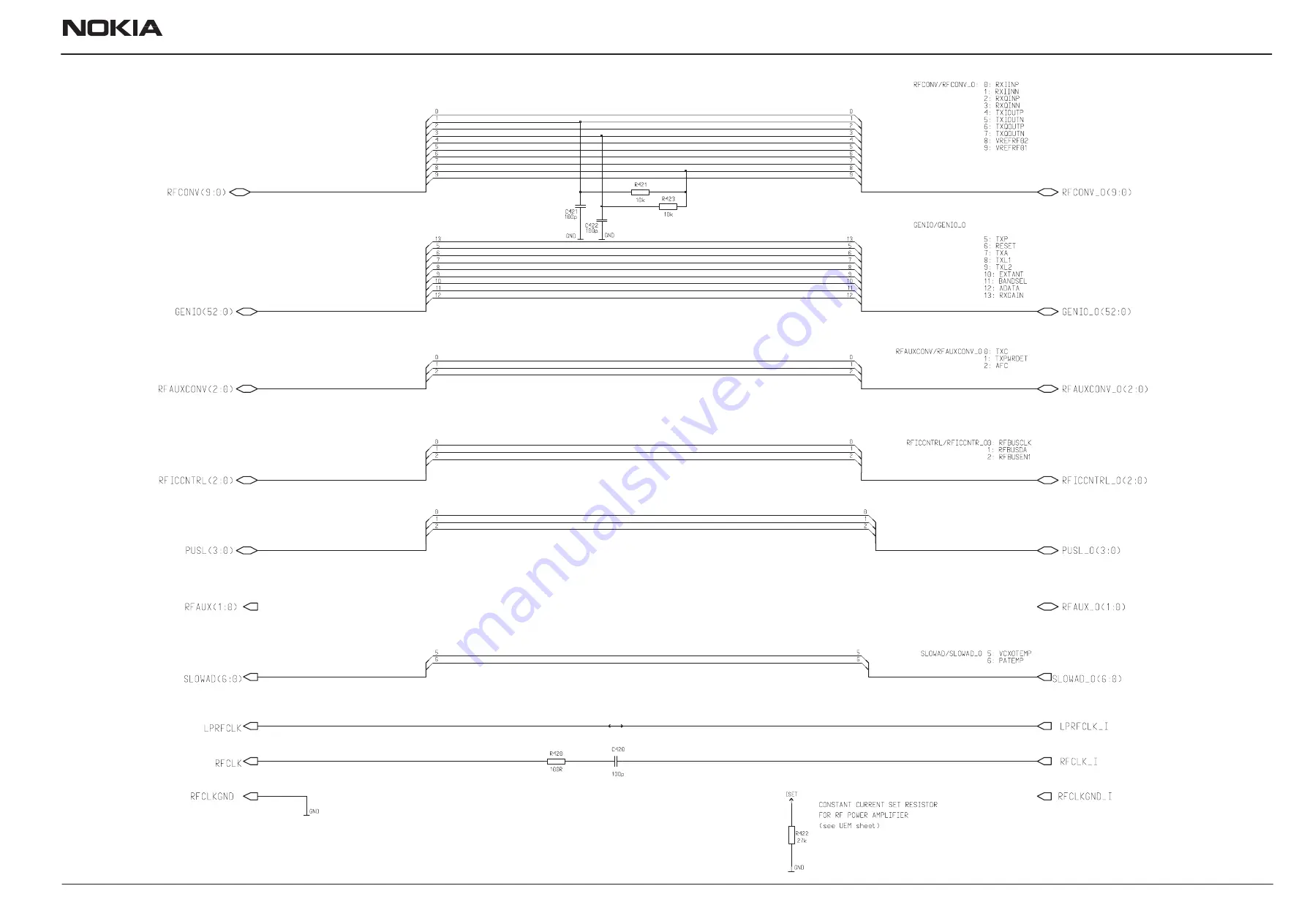
Page 206: ...NHM 7 System Module LA5 PAMS Technical Documentation B 13 Issue 1 10 2001 Nokia Corporation GSM RF BB Interface Version 1 3 Edit 35 for layout version 17 ...
Page 207: ...NHM 7 System Module LA5 PAMS Technical Documentation B 14 Issue 1 10 2001 Nokia Corporation Flash Memory Version 2 0 Edit 32 for layout version 17 ...
Page 208: ...NHM 7 System Module LA5 PAMS Technical Documentation B 15 Issue 1 10 2001 Nokia Corporation Layout Diagram of LA5 Top Version 17 Layout Diagram of LA5 Bottom Version 17 ...
Page 209: ...NHM 7 System Module LA5 PAMS Technical Documentation B 16 Issue 1 10 2001 Nokia Corporation Testpoints of LA5 Top Version xx Testpoints of LA5 Bottom Version 17 ...
Page 210: ...NHM 7 System Module LA5 PAMS Technical Documentation B 17 Issue 1 10 2001 Nokia Corporation UI Board LK5 for version 11 ...
Page 211: ...NHM 7 System Module LA5 PAMS Technical Documentation B 18 Issue 1 10 2001 Nokia Corporation Layout Diagram LK5 for version 11 ...
Page 212: ......