background image

Application Note

LMV771/LMV772/LMV774

The LMV771/LMV772/LMV774 are a family of precision am-
plifiers with very low noise and ultra low offset voltage.
LMV771/LMV772/LMV774's extended temperature range of
−40°C to 125°C enables the user to design this family of
products into a variety of applications including automotive.
The LMV771 has a maximum offset voltage of 1mV over the
extended temperature range. This makes the LMV771 ideal
for applications where precision is important.
The LMV772/LMV774 have a maximum offset voltage of 1mV
at room temperature and 1.2mV over the extended tempera-
ture range of −40°C to 125°C. Care must be taken when the
LMV772/LMV774 are designed into applications with heavy
loads under extreme temperature conditions. As indicated in
the DC tables, the LMV772/LMV774's gain and output swing
may be reduced at temperatures between 85°C and 125°C
with loads heavier than 2k

Ω.

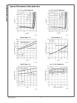
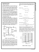
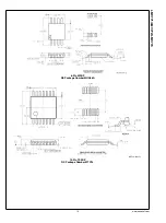
INSTRUMENTATION AMPLIFIER

Measurement of very small signals with an amplifier requires
close attention to the input impedance of the amplifier, gain
of the overall signal on the inputs, and the gain on each input
since we are only interested in the difference of the two inputs
and the common signal is considered noise. A classic solution
is an instrumentation amplifier. Instrumentation amplifiers
have a finite, accurate, and stable gain. Also they have ex-
tremely high input impedances and very low output
impedances. Finally they have an extremely high CMRR so
that the amplifier can only respond to the differential signal. A
typical instrumentation amplifier is shown in Figure 1.

20039636

FIGURE 1. Instrumentation Amplifier

There are two stages in this amplifier. The last stage, output
stage, is a differential amplifier. In an ideal case the two am-
plifiers of the first stage, input stage, would be set up as
buffers to isolate the inputs. However they cannot be con-
nected as followers because of real amplifier's mismatch.
That is why there is a balancing resistor between the two. The
product of the two stages of gain will give the gain of the in-
strumentation amplifier. Ideally, the CMRR should be infinite.
However the output stage has a small non-zero common
mode gain which results from resistor mismatch.

In the input stage of the circuit, current is the same across all
resistors. This is due to the high input impedance and low
input bias current of the LMV771. With the node equations we
have:

(1)

By Ohm’s Law:

(2)

However:

(3)

So we have:

(4)

Now looking at the output of the instrumentation amplifier:

(5)

Substituting from Equation 4:

(6)

This shows the gain of the instrumentation amplifier to be:

−K(2a+1)

Typical values for this circuit can be obtained by setting: a =
12 and K= 4. This results in an overall gain of −100.
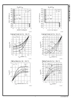
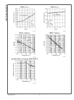
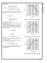
Figure 2 shows typical CMRR characteristics of this Instru-
mentation amplifier over frequency. Three LMV771 amplifiers
are used along with 1% resistors to minimize resistor mis-
match. Resistors used to build the circuit are: R

1

 = 21.6k

,

R

11

 = 1.8k

, R

2

 = 2.5k

 with K = 40 and a = 12. This results

in an overall gain of −1000, −K(2a+1) = −1000.

20039673

FIGURE 2. CMRR vs. Frequency

13

www.national.com

LMV771/LMV772/LMV774

Summary of Contents for LMV771

Page 1: ...tput swing into heavy loads The maximum input offset voltage for the LMV771 is 850 μV at room temperature and the input common mode voltage range includes ground The LMV771 is offered in the tiny SC70 5 package LMV772 in the space saving MSOP 8 and SOIC 8 and the LMV774 in TSSOP 14 Features Unless otherwise noted typical values at VS 2 7V Guaranteed 2 7V and 5V specifications Maximum VOS LMV771 85...

Page 2: ...specified all limits are guaranteed for TA 25 C V 2 7V V 0V VCM V 2 VO V 2 and RL 1MΩ Boldface limits apply at the temperature extremes Symbol Parameter Condition Min Note 7 Typ Note 6 Max Note 7 Units VOS Input Offset Voltage LMV771 0 3 0 85 1 0 mV LMV772 LMV774 0 3 1 0 1 2 TCVOS Input Offset Voltage Average Drift 0 45 µV C IB Input Bias Current Note 8 0 1 100 pA IOS Input Offset Current Note 8 0...

Page 3: ...y at the temperature extremes Symbol Parameter Condition Min Note 7 Typ Note 6 Max Note 7 Units VOS Input Offset Voltage LMV771 0 25 0 85 1 0 mV LMV772 LMV774 0 25 1 0 1 2 TCVOS Input Offset Voltage Average Drift 0 35 µV C IB Input Bias Current Note 8 0 23 100 pA IOS Input Offset Current Note 8 0 017 100 pA IS Supply Current Per Amplifier 600 950 960 µA CMRR Common Mode Rejection Ratio 0 5 VCM 3 5...

Page 4: ...fect reliability Note 4 Shorting output to V will adversely affect reliability Note 5 The maximum power dissipation is a function of TJ MAX θJA and TA The maximum allowable power dissipation at any ambient temperature is PD TJ MAX T A θJA All numbers apply for packages soldered directly into a PC board Note 6 Typical values represent the most likely parametric norm Note 7 All limits are guaranteed...

Page 5: ...Drawing SC70 5 LMV771MG A75 1k Units Tape and Reel MAA05A LMV771MGX 3k Units Tape and Reel 8 Pin SOIC LMV772MA LMV772MA 95 Units Rail M08A LMV772MAX 2 5k Units Tape and Reel 8 Pin MSOP LMV772MM A91A 1k Units Tape and Reel MUA08A LMV772MMX 3 5k Units Tape and Reel 14 Pin TSSOP LMV774MT LMV774MT 95 Units Rail MTC14 LMV774MTX 2 5k Units Tape and Reel 5 www national com LMV771 LMV772 LMV774 ...

Page 6: ...cs VOS vs VCM Over Temperature 20039627 VOS vs VCM Over Temperature 20039626 Output Swing vs VS 20039625 Output Swing vs VS 20039624 Output Swing vs VS 20039623 IS vs VS Over Temperature 20039630 www national com 6 LMV771 LMV772 LMV774 ...

Page 7: ...N vs VOUT 20039629 Sourcing Current vs VOUT Note 14 20039631 Sourcing Current vs VOUT Note 14 20039664 Sinking Current vs VOUT Note 14 20039632 Sinking Current vs VOUT Note 14 20039663 7 www national com LMV771 LMV772 LMV774 ...

Page 8: ...20039608 Input Bias Current Over Temperature 20039635 Input Bias Current Over Temperature 20039634 Input Bias Current Over Temperature 20039633 THD N vs Frequency 20039607 THD N vs VOUT 20039666 www national com 8 LMV771 LMV772 LMV774 ...

Page 9: ...quency Response Over Temperature 20039602 Open Loop Frequency Response 20039603 Open Loop Frequency Response 20039604 Open Loop Gain Phase with Cap Loading 20039605 Open Loop Gain Phase with Cap Loading 20039606 9 www national com LMV771 LMV772 LMV774 ...

Page 10: ...ignal Pulse Response 20039611 Non Inverting Small Signal Pulse Response 20039616 Non Inverting Large Signal Pulse Response 20039610 Non Inverting Small Signal Pulse Response 20039615 Non Inverting Large Signal Pulse Response 20039609 www national com 10 LMV771 LMV772 LMV774 ...

Page 11: ...ge Signal Pulse Response 20039614 Inverting Small Signal Pulse Response 20039620 Inverting Large Signal Pulse Response 20039613 Inverting Small Signal Pulse Response 20039618 Inverting Large Signal Pulse Response 20039612 11 www national com LMV771 LMV772 LMV774 ...

Page 12: ...Stability vs VCM 20039621 Stability vs VCM 20039622 PSRR vs Frequency 20039668 CMRR vs Frequency 20039665 Crosstalk Rejection vs Frequency LMV772 LMV774 20039694 www national com 12 LMV771 LMV772 LMV774 ...

Page 13: ... CMRR so that the amplifier can only respond to the differential signal A typical instrumentation amplifier is shown in Figure 1 20039636 FIGURE 1 Instrumentation Amplifier There are two stages in this amplifier The last stage output stage is a differential amplifier In an ideal case the two am plifiers of the first stage input stage would be set up as buffers to isolate the inputs However they ca...

Page 14: ...ressed as follows By KCL 7 Simplifying this further results in 8 or 9 Now substituting ω 2πf so that the calculations are in f Hz and not ω rad s and setting the DC gain HO R2 R1 and H VO Vi 10 Set fo 1 2πR1C 11 Low pass filters are known as lossy integrators because they only behave as an integrator at higher frequencies Just by looking at the transfer function one can predict the general form of...

Page 15: ...short circuit and the amplifier will have a constant high frequency gain of HO Figure 6 shows the transfer function of this high pass filter 20039658 FIGURE 6 Highpass Filter Transfer Function BAND PASS FILTER 20039660 FIGURE 7 Bandpass Filter Combining a low pass filter and a high pass filter will generate a band pass filter In this network the input impedance forms the high pass filter while the...

Page 16: ...ter The high pass signal is then fed into a low pass filter The outcome is a band pass signal meaning the second amplifier is a band pass filter This signal is then fed into the third amplifiers input and so the third am plifier behaves as a simple low pass filter 20039674 FIGURE 9 State Variable Active Filter The transfer function of each filter needs to be calculated The derivations will be more...

Page 17: ...es for the capacitors and re sistors Q reduces to or R5 10R6 R6 1 5kΩ R5 15kΩ Also for f 10kHz the center frequency is ωc 2πf 62 8kHz Using the expressions above the appropriate resistor values will be R2 R3 16kΩ The following graphs show the transfer function of each of the filters The DC gain of this circuit is 20039690 The frequency responses of each stage of the state variable active filter wh...

Page 18: ...Physical Dimensions inches millimeters unless otherwise noted SC70 5 NS Package Number MAA05A 8 Pin SOIC NS Package Number M08A www national com 18 LMV771 LMV772 LMV774 ...

Page 19: ...8 Pin MSOP NS Package Number MUA08A 14 Pin TSSOP NS Package Number MTC14 19 www national com LMV771 LMV772 LMV774 ...

Page 20: ...R INTELLECTUAL PROPERTY RIGHT LIFE SUPPORT POLICY NATIONAL S PRODUCTS ARE NOT AUTHORIZED FOR USE AS CRITICAL COMPONENTS IN LIFE SUPPORT DEVICES OR SYSTEMS WITHOUT THE EXPRESS PRIOR WRITTEN APPROVAL OF THE CHIEF EXECUTIVE OFFICER AND GENERAL COUNSEL OF NATIONAL SEMICONDUCTOR CORPORATION As used herein Life support devices or systems are devices which a are intended for surgical implant into the bod...

Reviews: