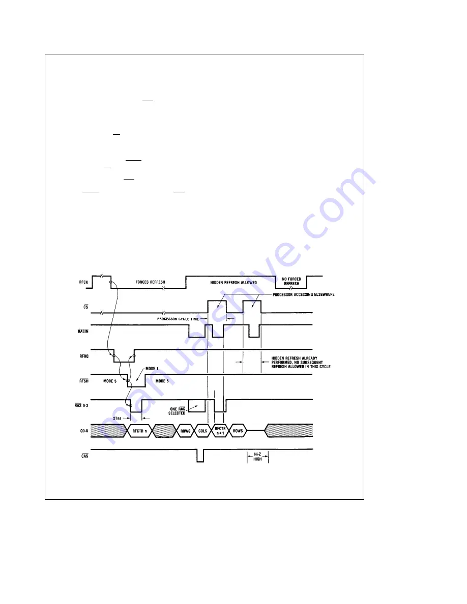
background image

Refreshing

The DP8409A also provdes hidden refresh capability while
in one of the automatic access modes (

Figure 4 ). In this

mode, it will automatically perform a refresh without the sys-
tem being interrupted. To do this, the DP8409A requires two
clock signals, refresh clock (RFCK) which defines the re-
fresh period (usually 16

m

s), and RAS generator clock

(RGCK), which is typically the microprocessor clock.

Highest priority is given to hidden refreshing through use of
level sensing of RFCK. A refresh cycle begins when RFCK
transitions to a high level. If during the time RFCK is high the
DP8409A is deselected (CS in the high state) and the proc-
essor is accessing another portion of the system such as
another memory segment, or ROM, or a peripheral, then a
hidden refresh is performed. When a read or write cycle is
initiated by the processor, the RASIN input on the DP8409A
transitions low. With CS high, this causes the present state
of the internal refresh counter to be placed on the address
outputs, followed by the four RAS outputs transitioning low,
strobing the refresh address into the DRAM array. When the
cycle ends, RASIN will terminate, thus forcing the RAS out-
puts back to their inactive state and ending the hidden re-
fresh. The refresh counter is then incremented and another
microprocssor cycle can begin immediately. However, to
save power, the DP8409A will allow only one hidden refresh
to occur during a given RFCK cycle.

In the event that a hidden refresh does not occur, the
DP8409A must force a refresh before the RFCK’s next
positive-going transition. The system is notified after the nega-
tive-going RFCK transition that a hidden refresh has not oc-

curred, via the refresh request output (RF I/O pin). The sys-
tem acknowledges the request for a forced refresh by set-
ting M2 (refresh) low on the DP8409A and preventing fur-
ther access to the DP8409A. The DP8409A then uses
RGCK to generate an automatic forced refresh. The refresh
request pin then returns to the inactive state, and the
DP8409A allows the processor to take full system control
after the forced refresh has been completed.

OCTAL MEMORY DRIVERS

For those applications where the memory array is extremely
large or the controller design is unique to a particular appli-
cation requirement, specialized high capacitive load ad-
dress and control buffers are required. However, like any
other element in a DRAM system, selection of the improper
driver can have significant impact on system performance.

In the past, this function has been performed using Schottky
logic family circuits such as the DM74S240 octal inverter or
the DM74S244 octal buffer. The output stages of these de-
vices have good drive capability, but their performance with
heavy capacitive loads is not ideal for DRAM arrays. The
key disadvantage of these devices is their non-symmetrical
rise and fall time characteristics and their long propagation
delays with heavy load capacitance. The former is a result
of impedance mismatch in the upper and lower output
stages. The latter stems from process capability and circuit
design techniques not tailored to the DRAM application.
The combined result of all these factors is increased output
skew in address and control lines when these devices are
used as buffers.

TL/F/5012 – 4

FIGURE 4. Hidden and Forced Refresh Timing of the DP8409A

4

Summary of Contents for DP8400

Page 1: ... dynamic RAM controller driver was the first controller to resolve all of these problems This Schottky bipolar device provides the flexibility of external access control along with automatic access timing genera tion without the need for an external timing generator clock In addition on board capacitive drivers allow direct drive for over 88 DRAMs With the simple addition of refresh clocks the cir...

Page 2: ...nal clock is required On chip delays insure proper address and control sequenc ing once the valid parallel address is presented to the fall through input latches of the DP8409A When the RASIN transitions high to low the decoded RAS output transitions low strobing the row address into the DRAM array An on chip delay automatically generates a guaranteed selectable mode 5 or 6 row address hold time A...

Page 3: ...ershoot undershoot at memories TL F 5012 2 FIGURE 2 Typical Application of DP8409A Using External Control and Refresh in Modes 0 and 4 TL F 5012 3 FIGURE 3 This figure demonstrates the automatic accessing capability of the DP8409A Only one strobing edge RASIN is required for generation of all DRAM access timing signals This is accomplished with on chip delay generators eliminating the need for ext...

Page 4: ...sition Thesystemisnotifiedafterthenega tive going RFCK transition that a hidden refresh has not oc curred via the refresh request output RF I O pin The sys tem acknowledges the request for a forced refresh by set ting M2 refresh low on the DP8409A and preventing fur ther access to the DP8409A The DP8409A then uses RGCK to generate an automatic forced refresh The refresh request pin then returns to...

Page 5: ... a reasonable level as demonstrated by the graphs shown in Figures 7a 7b of power versus frequency The DP84240 and the DP84244 are fabricated on a high performance oxide isolated Schottky bipolar process Spe cial circuit techiques have been used to minimize internal delays and skews Additionally both rise and fall time char acteristics track closely as a function of load capacitance This has been ...

Page 6: ...to input pulse distortion ERROR CORRECTION The determination of whether a DRAM system requires er ror correction must be resolved early in the system design A positive answer to this question may have far reaching impact on board development time and component cost It is clear however that such a decision cannot be taken lightly The type and origin of errors in DRAM systems are many and can result...

Page 7: ... read memory access cycles Figure 9a shows the normal write cycle where system data is used by the DP8400 to generate parity bits called check bits based on certain combinations of the data bits This combination is defined by the DP8400 s matrix shown in Figure 10 When ever a 1 occurs in any row the corresponding input data bit at the top of the column helps determine the parity for that check bit...

Page 8: ...P8400 TL F 5012 12 FIGURE 9b Normal Read Mode Using the Error Monitoring Method with the DP8400 TL F 5012 13 FIGURE 9c Normal Read Mode Using the Always Correct Method with the DP8400 C2 C3 generate odd parity TL F 5012 14 FIGURE 10 DP8400 Matrix 8 ...

Page 9: ...ould not be quickly found The occurrence of a double error comprising one soft and one hard must now be considered This type of error has a higher probability than two soft errors The hard error may be due to a catastrophic chip failure and a subsequent soft error will create two errors This can be a source of concern since most error correction chips cannot handle double er rors of this type Ther...

Page 10: ...n the system to warn the operator that the system is in a degrad ed operational mode and that field service should occur shortly In the meantime the system will continue to operate properly The key to the effectiveness of the DP8400 in this application is its three error flags which allow complete error reportingÐincluding a unique double error indication DP8402A 3 4 5 32 Bit Error Detector and Co...

Page 11: ... the system can implement byte writing to the DRAM array This system structure requires the insertion of few or no wait states during a memory access cycle thus maximizing throughput The DP84XX2 circuits have been designed to work with all of National s DRAM controller drivers to con trol refreshing so that system throughput is affected only when absolutely necessary First in any refresh clock per...

Page 12: ...urers CPU enjoying a favorite role Data sheets and more detailed application information are available for all the members of the DP8400 family Contact your local National Semiconductor representative or Nation al Semiconductor directly TL F 5012 18 FIGURE 14 Flexible Application of the DP8409A and DP8400 This Figure Shows an Application with a 16 Bit Microprocessor TABLE VII The DP84300 Series of...

Page 13: ...13 ...

Page 14: ...h instructions for use provided in the labeling can effectiveness be reasonably expected to result in a significant injury to the user National Semiconductor National Semiconductor National Semiconductor National Semiconductor Corporation Europe Hong Kong Ltd Japan Ltd 1111 West Bardin Road Fax a49 0 180 530 85 86 13th Floor Straight Block Tel 81 043 299 2309 Arlington TX 76017 Email cnjwge tevm2 ...

Reviews: