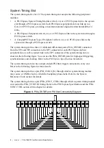
An independent buffer drives PXIe_CLK100 to each peripheral slot. These clocks are matched
in skew to less than 100 ps. The differential pair must be terminated on the peripheral with
LVPECL termination for the buffer to drive PXIe_CLK100 so that when there is no peripheral
or a peripheral that does not connect to PXIe_CLK100, there is no clock being driven on the
pair to that slot.
An independent buffer drives PXIe_SYNC100 to each peripheral slot. The differential pair
must be terminated on the peripheral with LVPECL termination for the buffer to drive
PXIe_SYNC100 so that when there is no peripheral or a peripheral that does not connect to
PXIe_SYNC100, there is no SYNC100 signal being driven on the pair to that slot.
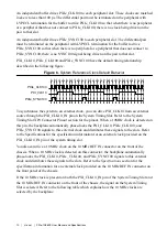
PXI_CLK10, PXIe_CLK100 and PXIe_SYNC100 have the default timing relationship
described in the following figure.
Figure 6. System Reference Clock Default Behavior
PXIe_CLK100
PXI_CLK10
PXIe_SYNC100
0 1 2 3 4 5 6 7 8 9 0 1 2 3 4 5 6 7 8 9 0 1 2 3 4 5 6 7 8 9
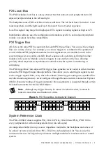
To synchronize the system to an external clock, you can drive PXI_CLK10 from an external
source through the PXI_CLK10_IN pin on the System Timing Slot. Refer to the System
Timing Slot XP4 Connector Pinout section for the pinout. When a 10MHz clock is detected on
this pin, the backplane automatically phase-locks the PXI_CLK10, PXIe_CLK100, and
PXIe_SYNC100 signals to this external clock and distributes these signals to the slots. Refer
to the Specifications for the specification information for an external clock provided on the
PXI_CLK10_IN pin of the system timing slot.
You also can drive a 10 MHz clock on the 10 MHz REF IN connector on the front of the
chassis. When a 10 MHz clock is detected on this connector, the backplane automatically
phase-locks the PXI_CLK10, PXIe_CLK100, and PXIe_SYNC100 signals to this external
clock and distributes these signals to the slots. Refer to the
Specifications
section for the
specification information for an external clock provided on the 10 MHz REF IN connector on
the front panel of the chassis.
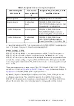
If the 10 MHz clock is present on both the PXI_CLK10_IN pin of the System Timing Slot and
the 10 MHz REF IN connector on the front of the chassis, the signal on the System Timing
Slot is selected. Refer to the following table which explains how the 10 MHz clocks are
selected by the backplane.
10
|
ni.com
|
PXIe-1086DC User Manual and Specifications


