background image

3-10

3-11

BIOS Setup  

MS-98L1   


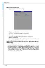
Launch OnBoard LAN OpROM

These  settings  enable/disable  the  initialization  of  the  onboard/onchip  LAN 

Boot ROM during bootup. Selecting [Disabled] will speed up the boot process.


GPIO Group Configuration


GPO0 ~ GPO7

These settings control the operation mode of the specified GPIO.

Summary of Contents for MS-98L1

Page 1: ...i MS 98L1 v1 x Industrial Computer Board ...

Page 2: ...ve owners No warranty as to accuracy or completeness is expressed or implied MSI reserves the right to make changes to this document without prior notice Revision History Revision Date V1 0 2019 07 Technical Support If a problem arises with your product and no solution can be obtained from the user s manual please contact your place of purchase or local distributor Alternatively please visit https...

Page 3: ...t place anything over the power cord Always Unplug the Power Cord before inserting any add on card or module All cautions and warnings on the equipment should be noted Never pour any liquid into the opening that could damage or cause electrical shock If any of the following situations arises get the equipment checked by service personnel The power cord or plug is damaged Liquid has penetrated into...

Page 4: ...ed household waste Please use the public collection system to return recycle or treat them in compliance with the local regulations 廢電池請回收 Taiwan For better environmental protection waste batteries should be collected separately for recycling or special disposal California USA The button cell battery may contain perchlorate material and requires special handling when recycled or disposed of in Cal...

Page 5: ... or more of the measures listed below Reorient or relocate the receiving antenna Increase the separation between the equipment and receiver Connect the equipment into an outlet on a circuit different from that to which the receiver is connected Consult the dealer or an experienced radio television technician for help Notice 1 The changes or modifications not expressly approved by the party respons...

Page 6: ...nce Statement v WEEE Statement v 1 Overview 1 1 Specifications 1 2 Layout 1 6 Rear Panel I O Options 1 7 2 Hardware Setup 2 1 Components Reference Guide 2 2 CPU Central Processing Unit 2 4 Memory 2 7 Storage 2 9 Power Supply 2 11 Rear Panel I O 2 13 Connectors 2 15 Jumpers 2 21 Slots 2 22 3 BIOS Setup 3 1 Entering Setup 3 2 The Menu Bar 3 4 Main 3 5 Advanced 3 6 Boot 3 12 Security 3 13 Chipset 3 2...

Page 7: ...vii MS 98L1 Appendix GPIO WDT BKL Programming A 1 Abstract A 2 General Purposed IO A 3 Watchdog Timer A 4 LVDS Backlight Brightness Control A 5 SMBus Access A 6 ...

Page 8: ......

Page 9: ...S 98L1 an excellent industrial computer board Based on the innovative Intel Coffee Lake S Coffee Lake S Refresh Processor the MS 98L1 is engineered to provide reliable performance for a wide variety of industrial applications 1 Overview ...

Page 10: ...um 95W Intel Core i7 8700 i7 8700T Intel Core i5 8500 i5 8500T Intel Core i3 8100 i3 8100T Intel Pentium G5400 5400T Intel Celeron G4900 G4900T SKU2 Q370 SKU3 H310 SKU4 H310 support 9th Gen Intel Coffee Lake S Refresh Embedded IOTG Processors Maximum 65W Intel Core i7 9700E i7 9700TE Intel Core i5 9500E i5 9500TE Intel Core i3 9100E i3 9100TE PCH Intel C246 Q370 H310 Express Chipset Memory 2 DDR4 ...

Page 11: ...2 DisplayPort Max resolution 4096x2304 60Hz DP supported 1 HDMI Max resolution 4096x2160 24Hz co lay DP 1 LVDS 18 24 bit Dual Channel Max resolution 1920x1200 60Hz Expansion Slot 1 PCIe 3 0 x16 slot 1 Mini PCIe slot 1 Nano SIM holder For SKU1 SKU2 1 M 2 E Key 2230 slot with PCIe x1 USB 2 0 signal For SKU1 SKU2 Rear Panel I O 1 3 port audio connector Line in Line Out Mic in 2 DisplayPorts 1 HDMI po...

Page 12: ...usion Header 1 LVDS Box Header for SKU1 SKU2 1 LVDS Inverter Box Header for SKU1 SKU2 1 SMBus Box Header for SKU1 SKU2 1 Amplifier Box Header for SKU1 SKU2 1 S PDIF Box Header for SKU1 SKU2 1 LVDS Power Jumper for SKU1 SKU2 1 LVDS Inverter Power Jumper for SKU1 SKU2 3 COM Port Power Jumpers for SKU1 SKU2 SKU3 1 COM Port Power Jumper for SKU4 1 Clear CMOS Jumper 1 AT ATX Jumper 1 USB Switch Jumper ...

Page 13: ...9 LM 1 Intel I211 AT Internal I O LVDS Yes COM 2 RS232 422 485 4 RS232 1 RS232 422 485 3 RS232 1 RS232 422 485 1 RS232 USB 2 0 2 USB 3 1 Gen 1 2 4 signal shared with Rear USB 3 1 Gen 1 TPM2 0 Onboard Expansion box header SATA 3 0 3 M 2 M Key with SATA PCIe x4 signal with SATA signal M 2 E Key with PCIe x1 USB 2 0 signal Intel AC9260 AC9560 WiFi 802 11ac Bluetooth 5 0 CNVi supported No Support for ...

Page 14: ...LVDS Power Jumper Chassis Intrusion Header M 2 M Key Slot LVDS Inverter Power Jumper USB Switch Jumper ME Jumper S PDIF Box Header SO DIMM Slot SATA 3 0 Connector LVDS Box Header SMBus Box Header Amplifier Box Header ATX Power Connector Rear Panel I O CPU Fan Connector PCIe Slot ATX Power Connector M 2 E Key Slot USB 3 1 Gen 1 Connector COM Port Power Jumper PCIe Jumper Nano SIM Holder backside TP...

Page 15: ... Line In Line Out Mic In SKU2 Q370 HDMI DP by option DisplayPort GbE LAN USB 3 1 Gen 2 USB 3 1 Gen 1 Line In Line Out Mic In SKU3 H310 HDMI DP by option DisplayPort GbE LAN USB 3 1 Gen 1 USB 2 0 GbE LAN Line In Line Out Mic In SKU4 H310 HDMI DP by option DisplayPort GbE LAN USB 3 1 Gen 1 USB 2 0 Line In Line Out Mic In ...

Page 16: ......

Page 17: ...allation be careful in holding the components and follow the installation procedures For some components if you install in the wrong orientation the components will not work properly Use a grounded wrist strap before handling computer components Static electricity may damage the components 2 Hardware Setup ...

Page 18: ...SMB1 JSPDIF1 BAT1 JAMP1 JUSBD2 JCMOS1 M2_E1 JCASE1 DIMM1 DIMM2 JUSBD1 JUSB1 JUSB2 JUSB3 JUSB4 SYSFAN1 CPUFAN1 JPWR2 JLVDS1 PCIE1 JME_DIS1 JCOM2 JCOM1 JGPIO1 JCOM3 JFP1 JCOMP1 JCOMP3 JCOMP2 JATX1 SATA1 SATA3 SATA2 MINIPCIE1 J_CFG1 JVDD1 JINVT1 JINV1 M2_M1 ...

Page 19: ... JGPIO1 2 15 Front Panel Connector JFP1 2 16 Chassis Intrusion Header JCASE1 2 16 LVDS Box Header JLVDS1 For SKU1 SKU2 2 17 LVDS Inverter Box Header JINVT1 For SKU1 SKU2 2 17 COM Port Box Headers JCOM1 JCOM2 JCOM3 Optional 2 18 Amplifier Box Header JAMP1 For SKU1 SKU2 2 19 S PDIF Box Header JSPDIF1 For SKU1 SKU2 2 19 SMBus Box Header JSMB1 For SKU1 SKU2 2 19 USB 2 0 Box Header JUSB4 For SKU1 SKU2 ...

Page 20: ...rly to protect the CPU from overheating Make sure that you apply an even layer of thermal paste or thermal tape between the CPU and the heatsink to enhance heat dissipation Replacing the CPU While replacing the CPU always turn off the power supply or unplug the power supply s power cord from the grounded outlet first to ensure the safety of CPU Introduction to LGA 115x CPU The surface of LGA 115x ...

Page 21: ...ver and remove the plastic cap 2 Lift the load lever up to fully open position 3 After confirming the CPU direction for correct mating put down the CPU in the socket housing frame Be sure to grasp on the edge of the CPU base Note that the alignment keys are matched 4 Engage the load lever while pressing down lightly onto the load plate Alignment Key Important Visually inspect if the CPU is seated ...

Page 22: ...the cooler Turn over the motherboard to confirm that the clip ends are correctly inserted 8 Finally attach the CPU Fan cable to the CPU fan connector on the motherboard Important Confirm if your CPU cooler is firmly installed before turning on your system Do not touch the CPU socket pins to avoid damage Whenever CPU is not installed always protect your CPU socket pins with the plastic cap covered ...

Page 23: ...sity in different channel DIMM slots Recommended Memory Population Number of DIMMs installed 1 2 DIMM1 ch A V V DIMM2 ch B V Important V indicates a populated DIMM slot Paired memory installation for Max performance Populate the same DIMM type in each channel specifically 1 Use the same DIMM size 2 Use the same number of ranks per DIMM ...

Page 24: ...m that will only allow it to fit one way into the slot Push the SO DIMM deeply into the slot The side clips of the slot will automatically close when the SO DIMM is properly seated and an audible click should be heard 3 Manually check if the SO DIMM has been locked in place by the slot s side clips Important You can barely see the golden finger if the SO DIMM is properly inserted in the DIMM slot ...

Page 25: ...46 SKU2 Q370 SKU3 H310 SKU4 H310 SATA 3 SATA 6Gb s ports RAID 0 1 5 10 supported RAID 10 should configured with M 2 AHCI Mode supported 3 SATA 6Gb s ports AHCI Mode supported M 2 M Key 1 M 2 M Key 2242 2280 slot with SATA PCIe x4 signal 1 M 2 M Key 2242 2280 slot with SATA signal ...

Page 26: ... Serial ATA device Important Please do not fold the SATA cable into a 90 degree angle Otherwise data loss may occur during transmission M2_M1 M 2 M Key 2242 2260 2280 Slot for SSD Please install the M 2 solid state drive SSD into the M 2 slot as shown below Important Intel RST only supports PCIe M 2 SSD with UEFI ROM and does not support Legacy ROM ...

Page 27: ...2 11 MS 98L1 Power Supply JPWR1 JPWR2 Power Connectors JPWR1 JPWR2 These connectors allow you to connect a power supply 5 1 8 4 JPWR2 1 Ground 5 12V 2 Ground 6 12V 3 Ground 7 12V 4 Ground 8 12V ...

Page 28: ...e all power connectors are connected to the power supply to ensure stable operation of the motherboard Make sure that you hold the onboard power connector firmly before disconnecting the power cable To avoid some issues like system instability reset and shutdown caused by energy insufficient power supply we suggest you should follow Intel Power Supply Design Guide Rev 1 4 list and Intel Document N...

Page 29: ...e In Line Out Mic In SKU2 Q370 HDMI DP by option DisplayPort GbE LAN USB 3 1 Gen 2 USB 3 1 Gen 1 Line In Line Out Mic In SKU3 H310 HDMI DP by option DisplayPort GbE LAN USB 3 1 Gen 1 USB 2 0 GbE LAN Line In Line Out Mic In SKU4 H310 HDMI DP by option DisplayPort GbE LAN USB 3 1 Gen 1 USB 2 0 Line In Line Out Mic In ...

Page 30: ...ort USB 3 1 Gen 2 the SuperSpeed USB 10Gbps delivers high speed data transfer for various devices such as storage devices hard drives video cameras etc h h USB 3 1 Gen 1 Port USB 3 1 Gen 1 the SuperSpeed USB delivers up to 5Gbps high speed data transfer for various devices such as storage devices hard drives video cameras etc h h USB 2 0 Port The USB Universal Serial Bus port is for attaching USB ...

Page 31: ...GND If the motherboard has a System Hardware Monitor chipset onboard you must use a specially designed fan with speed sensor to take advantage of the fan control 4 1 CPUFAN1 SYSFAN1 1 GND 2 FAN POWER 3 FAN SENSE 4 FAN_PWM GPIO DIO Connector JGPIO1 This connector is provided for the General Purpose Input Output GPIO peripheral module 1 2 19 20 JGPIO1 1 GND 2 GND 3 GPO0 4 GPI0 5 GPO1 6 GPI1 7 GPO2 8...

Page 32: ...SW PW SW Key 2 4 6 8 10 1 3 5 7 9 HDD LED HDD LED Reser SW Reset SW NC LED Voltage V Current mA Power 5 18 51 HDD 5 18 51 Chassis Intrusion Header JCASE1 This connector connects to the chassis intrusion switch cable If the computer case is opened the chassis intrusion mechanism will be activated The system will record this intrusion and a warning message will flash on screen To clear the warning y...

Page 33: ...3 BKLT_EN 6 GND 40 2 39 1 JLVDS1 1 12V 2 12V 3 LCD_VDD 4 12V 5 LCD_VDD 6 LCD_VDD 7 LVDS_DDC_CLK 8 LVDS_DDC_DATA 9 BKLT_CTRL 10 LVDS_VDD_EN 11 BKLT_EN 12 LVDS_DETECT 13 LVDSA_DATA1 14 LVDSA_DATA0 15 LVDSA_DATA1 16 LVDSA_DATA0 17 GND 18 GND 19 LVDSA_DATA3 20 LVDSA_DATA2 21 LVDSA_DATA3 22 LVDSA_DATA2 23 GND 24 GND 25 LVDSB_DATA1 26 LVDSB_DATA0 27 LVDSB_DATA1 28 LVDSB_DATA0 29 GND 30 GND 31 LVDSB_DATA...

Page 34: ...OM Port Box Header JCOM1 JCOM2 JCOM3 JCOM1 JCOM2 JCOM1 1 2 19 20 JCOM2 JCOM3 RS232 1 2 DCD 3 4 RXD 5 6 TXD 7 8 DTR 9 10 GND 11 12 DSR 13 14 RTS 15 16 CTS 17 18 RI POWER 19 20 NC 1 2 19 20 JCOM1 RS232 RS422 RS485 1 2 DCD 1 2 TXD 1 2 TXD 3 4 RXD 3 4 TXD 3 4 TXD 5 6 TXD 5 6 RXD 5 6 NC 7 8 DTR 7 8 RXD 7 8 NC 9 10 GND 9 10 GND 9 10 GND 11 12 DSR 11 12 NC 11 12 NC 13 14 RTS 13 14 NC 13 14 NC 15 16 CTS 1...

Page 35: ...KU1 SKU2 This pinheader is used to connect S PDIF Sony Philips Digital Interconnect Format interface for digital audio transmission 1 4 JAMP1 1 AMP_L 2 AMP_L 3 AMP_R 4 AMP_R 3 1 JSPDIF1 1 5V 2 SPDIF 3 GND SMBus Box Header JSMB1 For SKU1 SKU2 This connector is provided for users to connect System Management Bus SMBus interface 4 1 JSMB1 1 5V 2 CLK 3 DATA 4 GND ...

Page 36: ...USB3 1 USB3_PWR 11 USB2_DP2 2 USB3_RX1N 12 USB2_DN2 3 USB3_RX1P 13 GND 4 GND 14 USB3_TX2P 5 USB3_TX1N 15 USB3_TX2N 6 USB3_TX1P 16 GND 7 GND 17 USB3_RX2P 8 USB2_DN1 18 USB3_RX2N 9 USB2_DP1 19 USB3_PWR 10 NA 20 NA 7 1 8 2 JUSB4 1 5V 2 GND 3 USB_D 4 USB_D 5 USB_D 6 USB_D 7 GND 8 5V Important Note that the pins of VCC and GND must be connected correctly to avoid possible damage To use a USB3 1 device ...

Page 37: ...2 JATX1 J_CFG1 JVDD1 JINV1 Jumper Name Default Setting Description JCMOS1 1 1 2 Normal 2 3 Clear CMOS JATX1 1 1 2 ATX 2 3 AT JME_DIS1 1 1 2 Normal 2 3 ME Disable JCOMP1 6 5 2 1 1 2 5V 3 4 12V 5 6 RI JCOMP2 JCOMP3 1 1 2 5V 2 3 12V J_CFG1 1 1 2 1 x16 PCIe 2 3 2 x8 PCIe JVDD1 1 1 2 3V 2 3 5V JINV1 1 1 2 5V 2 3 12V JUSBD1 JUSBD2 1 1 2 Rear I O 2 3 Internal I O ...

Page 38: ... cards M2_E1 M 2 E Key 2230 Slot for WiFi BT For SKU1 SKU2 Please install the Wi Fi Bluetooch card into the M 2 slot as shown below Nano SIM Holder For SKU1 SKU2 This holder is provided for 3G 4G LTE WiFi BT CANBus Nano SIM cards Important When adding or removing expansion cards make sure that you unplug the power supply first Meanwhile read the documentation for the expansion card to configure an...

Page 39: ... message appears on the screen at system startup and requests users to run SETUP Users want to change the default settings for customized features Important Please note that BIOS update assumes technician level experience As the system BIOS is under continuous update for better system performance the illustrations in this chapter should be held for reference only 3 BIOS Setup ...

Page 40: ...before you respond and you still wish to enter Setup restart the system by turning it OFF and On or pressing the RESET button You may also restart the system by simultaneously pressing Ctrl Alt and Delete keys Important The items under each BIOS category described in this chapter are under continuous update for better system performance Therefore the description may be slightly different from the ...

Page 41: ... a right pointer symbol appears to the left of certain fields that means a sub menu can be launched from this field A sub menu contains additional options for a field parameter You can use arrow keys to highlight the field and press Enter to call up the sub menu Then you can use the control keys to enter values and move from field to field within a sub menu If you want to return to the main menu j...

Page 42: ...specify the priority of boot devices Security Use this menu to set supervisor and user passwords Chipset This menu controls the advanced features of the onboard chipsets Power Use this menu to specify your settings for power management Save Exit This menu allows you to load the BIOS default values or factory default settings into the BIOS and exit the BIOS setup utility with or without changes ...

Page 43: ...ng allows you to set the system date The date format is Day Month Date Year System Time This setting allows you to set the system time The time format is Hour Minute Second SATA Mode Selection This setting specifies the SATA controller mode ...

Page 44: ...o the booting sequence This delay ensures that the logo is displayed for a sufficient amount of time Therefore it is recommended that you disable this BIOS feature for a faster boot up time Bootup NumLock State This setting is to set the Num Lock status when the system is powered on Setting to On will turn on the Num Lock key when the system is powered on Setting to Off will allow users to use the...

Page 45: ...n this way the system performance is highly improved If you disable the function the processor will use only one core to execute the instructions Please disable this item if your operating system doesn support HT Function or unreliability and instability may occur Intel R SpeedStep tm EIST EnhancedIntelSpeedStepTechnology allowsthesystemtodynamically adjust processor voltage and core frequency whi...

Page 46: ...Select Select an operation mode for the specified serial port FIFO Mode This setting controls the FIFO data transfer mode Shared IRQ Mode This setting provides the system with the ability to share interrupts among its serial ports Watch Dog Timer You can enable the system watch dog timer a hardware timer that generates a reset when the software that it monitors does not respond as expected each ti...

Page 47: ...and all fans speeds Smart Fan Configuration CPUFAN1 SYSFAN1 This setting enables disables the Smart Fan function Smart Fan is an excellent feature which will adjust the CPU system fan speed automatically depending on the current CPU system temperature avoiding the overheating to damage your system Type This setting specifies the fan type ...

Page 48: ...k boot PXE from BIOS PCI PCIE Device Configuration Legacy USB Support Set to Enabled if you need to use any USB 1 1 2 0 device in the operating system that does not support or have any USB 1 1 2 0 driver installed such as DOS and SCO Unix Audio Controller This setting enables disables the onboard audio controller ...

Page 49: ...se settings enable disable the initialization of the onboard onchip LAN Boot ROM during bootup Selecting Disabled will speed up the boot process GPIO Group Configuration GPO0 GPO7 These settings control the operation mode of the specified GPIO ...

Page 50: ...mpatibility Support Module a part of the Intel Platform Innovation Framework for EFI providing the capability to support legacy BIOS interfaces Boot Option Priorities This setting allows users to set the sequence of boot devices where BIOS attempts to load the disk operating system ...

Page 51: ...is Intrusion The field enables or disables the feature of recording the chassis intrusion status and issuing a warning message if the chassis is once opened Intel Trusted Execution Technology Intel Trusted Execution Technology provides highly scalable platform security in physical and virtual infrastructures Intel BIOS Guard Support Intel BIOS Guard Support ensures that updates to system BIOS flas...

Page 52: ...the Intel ME Management Engine ME State This setting enables disables the ME status Manageability Features State This setting enables disables the Manageability Features State AMT BIOS Features This setting enables disables the AMT BIOS Features AMT Configuration Intel Active Management Technology AMT is hardware based technology for remotely managing and securing PCs out of band ...

Page 53: ...ables disables Communications Hub Support JHI Support This setting enables disables support for Intel Dynamic Application Loader Host Interface JHI Core BIOS Done Message This setting enables disables Core BIOS Done Message sent to ME Firmware Update Configuration ME FW Image Re Flash This setting enables disables the ME FW image reflash ...

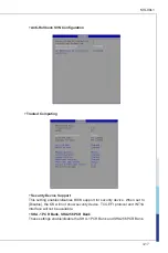
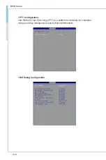
Page 54: ...3 16 BIOS Setup PTT Configuration Intel Platform Trust Technology PTT is a platform functionality for credential storage and key management used by Microsoft Windows ME Debug Configuration ...

Page 55: ...port This setting enables disables BIOS support for security device When set to Disable the OS will not show security device TCG EFI protocol and INT1A interface will not be available SHA 1 PCR Bank SHA256 PCR Bank These settings enable disable the SHA 1 PCR Bank and SHA256 PCR Bank ...

Page 56: ...ion Physical Presence Spec Version This settings show the TPM2 0 UEFI Spec Version and Physical Presence Spec Version TPM2 0 Interface Type This setting shows the TPM2 0 Interface Type Serial Port Console Redirection COM1 Console Redirection Console Redirection operates in host systems that do not have a monitor and keyboard attached This setting enables disables the operation of console redirecti...

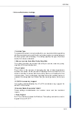
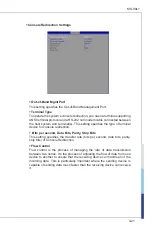
Page 57: ...the process of managing the rate of data transmission between two nodes It s the process of adjusting the flow of data from one device to another to ensure that the receiving device can handle all of the incoming data This is particularly important where the sending device is capable of sending data much faster than the receiving device can receive it VT UTF8 Combo Key Support This setting enables...

Page 58: ...r the POST has booted Serial Port for Out of Band Management Windows Emergency Management Services EMS Console Redirection Console Redirection operates in host systems that do not have a monitor and keyboard attached This setting enables disables the operation of console redirection When set to Enabled BIOS redirects and sends all contents that should be displayed on the screen to the serial COM p...

Page 59: ...ce for console redirection Bits per second Data Bits Parity Stop Bits This setting specifies the transfer rate bits per second data bits parity stop bits of Console Redirection Flow Control Flow control is the process of managing the rate of data transmission between two nodes It s the process of adjusting the flow of data from one device to another to ensure that the receiving device can handle a...

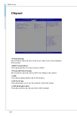
Page 60: ...s setting specifies the memory size for DVMT Primary IGFX Boot Display Use the field to select the primary IGFX boot display of the system LVDS This setting enables disables the LVDS interface LCD Panel Type This setting allows you to set the resolution of the LCD display LVDS Backlight Control This setting controls the intensity of the LVDS backlight ...

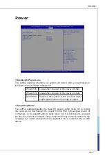
Page 61: ... Restores the system to the previous status before power failure or interrupt occurred Deep Sleep Mode The setting enables disables the Deep S5 power saving mode S5 is almost the same as G3 Mechanical Off except that the PSU still supplies power at a minimum to the power button to allow return to S0 A full reboot is required No previous content is retained Other components may remain powered so th...

Page 62: ...ivity or input signal of onchip LAN or USB devices is detected PCIE Ring PME This field specifies whether the system will be awakened from power saving modes when activity or input signal of onboard PCIE PCI Ring PME is detected RTC When Enabled your can set the date and time at which the RTC real time clock alarm awakens the system from suspend mode ...

Page 63: ...zed Defaults Use this menu to load the default values set by the motherboard manufacturer specifically for optimal performance of the motherboard Save as User Defaults Save changes as the user s default profile Restore User Defaults Restore the user s default profile Launch EFI Shell from filesystem device This setting helps to launch the EFI Shell application from one of the available file system...

Page 64: ......
Page 65: ...2 A 1 This appendix provides WDT Watch Dog Timer GPIO General Purpose Input Output and LVDS Backlight programming guide Appendix GPIO WDT BKL Programming ...

Page 66: ...ge provided for customer interest Inportb Outportb Inportl and Outportl are basic functions used for access IO ports and defined as following Inportb Read a single 8 bit I O port Outportb Write a single byte to an 8 bit port Inportl Reads a single 32 bit I O port Outportl Write a single long to a 32 bit port ...

Page 67: ...ample Set N_GPO0 output high val SMBus_ReadByte 0x6E 0x11 Read value from N_GPO0 port through SMBus val val 1 0 Set N_GPO0address bit 0 to 1 output high SMBus_WriteByte 0x6E 0x11 val Write back to N_GPO0 port through SMBus Example Set N_GPO1 output low val SMBus_ReadByte 0x6E 0x11 Read value from N_GPO1 port through SMBus val val 1 1 Set N_GPO1 address bit 1 to 0 output low SMBus_WriteByte 0x6E 0x...

Page 68: ... setting val Inportb WDT_BASE 0x05 Read current WDT setting val val 0x20 Enable WDT by set WD_EN bit 5 to 1 Outportb WDT_BASE 0x05 val Write back WDT setting 2 4 Disable WDT val Inportb WDT_BASE 0x05 Read current WDT setting val val 0xDF Disable WDT by set WD_EN bit 5 to 0 Outportb WDT_BASE 0x05 val Write back WDT setting 2 5 Check WDT Reset Flag If the system has been reset by WDT function this f...

Page 69: ...e 0xED into address 0x7F on SMBus device 0x42 2 Write desired backlight level from 0x0 30 to 0x10 100 into address 0x6E on SMBus device 0x42 Example Set LVDS backlight level to 0x10 100 SMBus_WriteByte 0x42 0x7F 0xED SMBus_WriteByte 0x42 0x6E 0x10 Set brightness to 100 3 2 Read the Level of LVDS Backlight 1 Write 0xED into address 0x7F on SMBus device 0x42 2 Read current backlight level from addre...

Page 70: ...FFSET from SMBus device DEVID Outportb LOWORD SMBUS_BASE 0xFE Outportb LOWORD SMBUS_BASE 0x04 DEVID 1 out Base 04 DEVID 1 Outportb LOWORD SMBUS_BASE 0x03 OFFSET out Base 03 OFFSET Outportb LOWORD SMBUS_BASE 0x02 0x48 out Base 02 48H mdelay 20 delay 20ms to let data ready while Inportl SMBUS_BASE 0x01 0 wait SMBus ready SMB_DATA Inportb LOWORD SMBUS_BASE 0x05 input Base 05 4 3 SMBus_WriteByte char ...

Reviews: