MPS MP1584 Manual Download Page 13

MP1584 – 3A, 1.5MHz, 28V STEP-DOWN CONVERTER 


MP1584 Rev. 1.0 

www.MonolithicPower.com 

13


8/8/2011 

MPS Proprietary Information. Unauthorized Photocopy and Duplication Prohibited. 


© 2011 MPS. All Rights Reserved. 

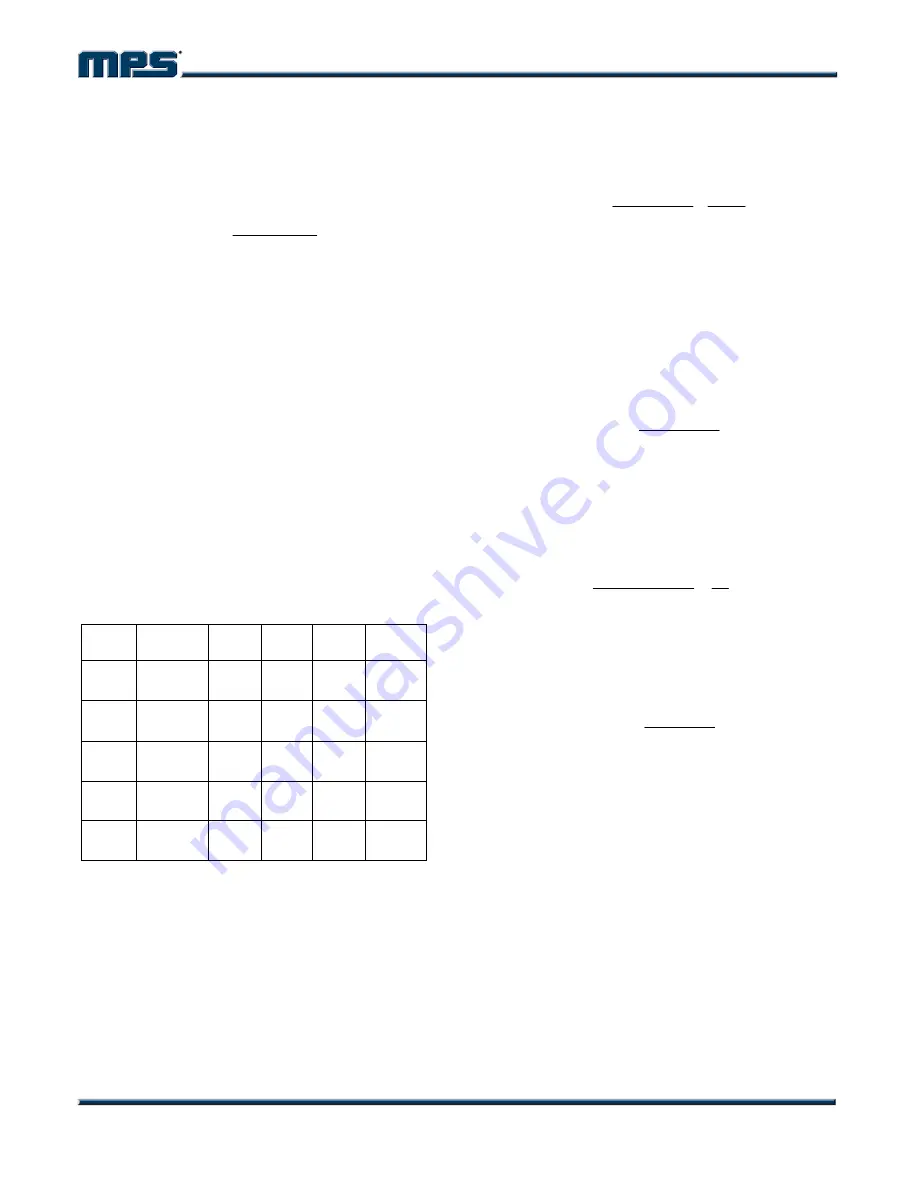
In this case (as shown in Figure 2), a third pole 
set by the compensation capacitor (C6) and the 
compensation resistor (R3) is used to 
compensate the effect of the ESR zero on the 
loop gain. This pole is located at: 

3

R

6

C

2

1

f

3

P


The goal of compensation design is to shape 
the converter transfer function to get a desired 
loop gain. The system crossover frequency 
where the feedback loop has the unity gain is 
important. Lower crossover frequencies result 
in slower line and load transient responses, 
while higher crossover frequencies could cause 
system unstable. A good rule of thumb is to set 
the crossover frequency to approximately one-
tenth of the switching frequency. The Table 3 
lists the typical values of compensation 
components for some standard output voltages 
with various output capacitors and inductors. 
The values of the compensation components 
have been optimized for fast transient 
responses and good stability at given conditions. 

Table 3—Compensation Values for Typical 
Output Voltage/Capacitor Combinations 

V

OUT


(V) 

L (µH) 

C2 

(µF) 

R3 

(k

C3 

(pF) 

C6 

1.8 4.7 47 

105 

100 

None 

2.5 

4.7 - 6.8 

22 

54.9 

220 

None 

3.3 6.8 

-10 22 68.1 220 None 

15 - 22 

22 

100 

150 

None 

12 

22 - 33 

22 

147 

150 

None 

To optimize the compensation components for 
conditions not listed in Table 3, the following 
procedure can be used.  

1. Choose the compensation resistor (R3) to set 
the desired crossover frequency. Determine the 
R3 value by the following equation: 

FB

OUT

CS

EA

C

V

V

G

G

f

2

C

2

3

R


Where f

is the desired crossover frequency.  

2. Choose the compensation capacitor (C3) to 
achieve the desired phase margin. For 
applications with typical inductor values, setting 
the compensation zero, f

Z1

, below one forth of 

the crossover frequency provides sufficient 
phase margin. Determine the C3 value by the 
following equation: 

C

f

3

R

2

4

3

C


3. Determine if the second compensation 
capacitor (C6) is required. It is required if the 
ESR zero of the output capacitor is located at 
less than half of the switching frequency, or the 
following relationship is valid: 

2

f

R

2

C

2

1

S

ESR


If this is the case, then add the second 
compensation capacitor (C6) to set the pole f

P3 

at the location of the ESR zero. Determine the 
C6 value by the equation: 

3

R

R

2

C

6

C

ESR


Summary of Contents for MP1584

Page 1: ...nt inductor current runaway during startup and thermal shutdown provides reliable fault tolerant operation By switching at 1 5MHz the MP1584 is able to prevent EMI Electromagnetic Interference noise p...

Page 2: ...y Voltage VIN 4 5V to 28V Output Voltage VOUT 0 8V to 25V Operating Junct Temp TJ 20 C to 125 C Thermal Resistance 4 JA JC SOIC8E 50 10 C W Notes 1 Exceeding these ratings may damage the device 2 The...

Page 3: ...VIN 28V 1 A Current Limit 4 0 4 7 A COMP to Current Sense Transconductance GCS 9 A V Error Amp Voltage Gain 5 200 V V Error Amp Transconductance ICOMP 3 A 40 60 80 A V Error Amp Min Source current VF...

Page 4: ...ied to this pin 4 FB Feedback This is the input to the error amplifier The output voltage is set by a resistive divider connected between the output and GND which scales down VOUT equal to the interna...

Page 5: ...VIN 12V VOUT 5V C1 10 F C2 22 F L1 10 H TA 25 C unless otherwise noted VSW 10V div VOUT AC Coupled 10mV div IL 1A div VSW 10V div VOUT AC Coupled 10mV div IL 1A div 1 v Steady State IOUT 0 1A fSW 500k...

Page 6: ...div Startup IOUT 0 1A 1ms div Shutdown IOUT 0 1A 5ms div Startup IOUT 1A Shutdown IOUT 1A 5ms div Startup IOUT 2A VOUT 2V div IL 1A div VSW 10V div VEN 5V div VOUT 2V div IL 1A div VSW 10V div VEN 5V...

Page 7: ...tion with current mode control for fast loop response and easy compensation It features a wide input voltage range internal soft start control and precision current limiting Its very low operational q...

Page 8: ...ect the chip from operating at insufficient supply voltage The UVLO rising threshold is about 3 0V while its falling threshold is a consistent 2 6V Internal Soft Start The soft start is implemented to...

Page 9: ...till the end of the turn on transition to avoid noise issues The comparator then compares the power switch current with the COMP voltage When the sensed current is higher than the COMP voltage the com...

Page 10: ...while being driven by the switched input voltage A larger value inductor will result in less ripple current that will result in lower output ripple voltage However the larger value inductor will have...

Page 11: ...put Rectifier Diode The output rectifier diode supplies the current to the inductor when the high side switch is off To reduce losses due to the diode forward voltage and recovery times use a Schottky...

Page 12: ...capacitors the ESR dominates the impedance at the switching frequency For simplification the output ripple can be approximated to ESR IN OUT S OUT OUT R V V 1 L f V V The characteristics of the outpu...

Page 13: ...and good stability at given conditions Table 3 Compensation Values for Typical Output Voltage Capacitor Combinations VOUT V L H C2 F R3 k C3 pF C6 1 8 4 7 47 105 100 None 2 5 4 7 6 8 22 54 9 220 None...

Page 14: ...inside the high di dt power loop If you have to do so the proper ground plane must be in place to isolate those Switching loss is expected to be increased at high switching frequency To help to improv...

Page 15: ...2011 MPS All Rights Reserved TYPICAL APPLICATION CIRCUITS C3 100pF C6 NS C4 100nF D1 VOUT 1 8V VIN 4 5V 28V VIN EN FREQ GND BST 5 8 1 4 3 7 2 6 SW FB COMP MP1584 EN Figure 3 1 8V Output Typical Appli...

Page 16: ...area formed by Input cap high side MOSFET and external switching diode 2 Bypass ceramic capacitors are suggested to be put close to the VIN Pin 3 Ensure all feedback connections are short and direct P...

Page 17: ...0 013 0 33 0 020 0 51 SEATING PLANE 0 000 0 00 0 006 0 15 0 051 1 30 0 067 1 70 TOP VIEW FRONT VIEW SIDE VIEW BOTTOM VIEW NOTE 1 CONTROL DIMENSION IS IN INCHES DIMENSION IN BRACKET IS IN MILLIMETERS 2...

Reviews: