M68360QUADS-040 Hardware User’s Manual
OPERATING INSTRUCTIONS
20
3.3.1
Main Memory Map
The memory map of devices that respond to User Data, User Program, Supervisory Data, Supervisory
Program, and DMA access is shown in TABLE 3-2.
NOTES:
1.
Refer to the MC68360 QUICC User’s Manual for complete description of the QUICC
internal memory.
2.
The device appears repeatedly in multiples of its size. For example, the Status Register
appears at memory locations 01230002, 01230006, 012300A etc...
3.
The DRAM SIMM installed in the M68360QUADS-040 is MCM36256 256Kx36 bit. The
user may replace the DRAM module with a higher density SIMM and increase the DRAM
space up to 8 MBytes.
a. For 68LC040 only, reserved otherwise
b. For 68LC040 only, reserved otherwise
a. Not populated - optional.
b. Connected to D0 - D15
100
00
MMU Table
Search
b
Code
All
101
0X
Supervisor Data
All
110
00
Supervisor Program
All
111
00
Supervisor CPU
QUICC’s MBAR register
111
11
Supervisor CPU
QUICC during interrupt acknowledge cycle.
TABLE 3-2 M68360QUADS-040 Main Memory Map
ADDESS RANGE
Accessed Device
Data Size
NOTES
00000000 - 001FFFFF
Flash PROM
32
2
00200000 - 003BFFFF
Empty Space
003C0000 - 003CFFFF
Bursting SRAM - BANK 1
a
32 + Parity
003E0000 - 003EFFFF
Bursting SRAM - BANK 2
32 + Parity
00400000 - 004FFFFF
00400000 - 005FFFFF
00400000 - 007FFFFF
00400000 - 00BFFFFF
DRAM SIMM MCM36256
DRAM SIMM MCM36512
DRAM SIMM MCM36100
DRAM SIMM MCM36200
32 + Parity
3
01210000 - 01211FFF
Slave QUICC Internal Memory
32
1
01230000 - 01231FFF
M68360QUADS-040 Status Register
16
b
2
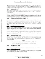
TABLE 3-1. EC040 Cycle Types and Responding Devices
TM(2:0)
TT(1:0)
Address Space
Responding Devices
F
re
e
sc
a
le
S
e
m
ic
o
n
d
u
c
to
r,
I
Freescale Semiconductor, Inc.
For More Information On This Product,
Go to: www.freescale.com
n
c
.
..

