background image

 2015 Microchip Technology Inc.


DS20005459B-page 33

Information contained in this publication regarding device
applications and the like is provided only for your convenience
and may be superseded by updates. It is your responsibility to
ensure that your application meets with your specifications.
MICROCHIP MAKES NO REPRESENTATIONS OR
WARRANTIES OF ANY KIND WHETHER EXPRESS OR
IMPLIED, WRITTEN OR ORAL, STATUTORY OR
OTHERWISE, RELATED TO THE INFORMATION,
INCLUDING BUT NOT LIMITED TO ITS CONDITION,
QUALITY, PERFORMANCE, MERCHANTABILITY OR
FITNESS FOR PURPOSE

Microchip disclaims all liability

arising from this information and its use. Use of Microchip
devices in life support and/or safety applications is entirely at
the buyer’s risk, and the buyer agrees to defend, indemnify and
hold harmless Microchip from any and all damages, claims,
suits, or expenses resulting from such use. No licenses are
conveyed, implicitly or otherwise, under any Microchip
intellectual property rights unless otherwise stated.

Trademarks

The Microchip name and logo, the Microchip logo, dsPIC, 
FlashFlex, flexPWR, JukeBlox, K

EE

L

OQ

, K

EE

L

OQ

 logo, Kleer, 

LANCheck, MediaLB, MOST, MOST logo, MPLAB, 
OptoLyzer, PIC, PICSTART, PIC

32

 logo, RightTouch, SpyNIC, 

SST, SST Logo, SuperFlash and UNI/O are registered 
trademarks of Microchip Technology Incorporated in the 
U.S.A. and other countries.

The Embedded Control Solutions Company and mTouch are 
registered trademarks of Microchip Technology Incorporated 
in the U.S.A.

Analog-for-the-Digital Age, BodyCom, chipKIT, chipKIT logo, 
CodeGuard, dsPICDEM, dsPICDEM.net, ECAN, In-Circuit 
Serial Programming, ICSP, Inter-Chip Connectivity, KleerNet, 
KleerNet logo, MiWi, motorBench, MPASM, MPF, MPLAB 
Certified logo, MPLIB, MPLINK, MultiTRAK, NetDetach, 
Omniscient Code Generation, PICDEM, PICDEM.net, PICkit, 
PICtail, RightTouch logo, REAL ICE, SQI, Serial Quad I/O, 
Total Endurance, TSHARC, USBCheck, VariSense, 
ViewSpan, WiperLock, Wireless DNA, and ZENA are 
trademarks of Microchip Technology Incorporated in the 
U.S.A. and other countries.

SQTP is a service mark of Microchip Technology Incorporated 
in the U.S.A.

Silicon Storage Technology is a registered trademark of 
Microchip Technology Inc. in other countries.

GestIC is a registered trademark of Microchip Technology 
Germany II GmbH & Co. KG, a subsidiary of Microchip 
Technology Inc., in other countries. 

All other trademarks mentioned herein are property of their 
respective companies.

© 2015, Microchip Technology Incorporated, Printed in the 
U.S.A., All Rights Reserved. 

ISBN: 978-1-5224-0039-4

Note the following details of the code protection feature on Microchip devices:

Microchip products meet the specification contained in their particular Microchip Data Sheet.

Microchip believes that its family of products is one of the most secure families of its kind on the market today, when used in the 
intended manner and under normal conditions.

There are dishonest and possibly illegal methods used to breach the code protection feature. All of these methods, to our 
knowledge, require using the Microchip products in a manner outside the operating specifications contained in Microchip’s Data 
Sheets. Most likely, the person doing so is engaged in theft of intellectual property.

Microchip is willing to work with the customer who is concerned about the integrity of their code.

Neither Microchip nor any other semiconductor manufacturer can guarantee the security of their code. Code protection does not 
mean that we are guaranteeing the product as “unbreakable.”

Code protection is constantly evolving. We at Microchip are committed to continuously improving the code protection features of our
products. Attempts to break Microchip’s code protection feature may be a violation of the Digital Millennium Copyright Act. If such acts
allow unauthorized access to your software or other copyrighted work, you may have a right to sue for relief under that Act.

Microchip received ISO/TS-16949:2009 certification for its worldwide 
headquarters, design and wafer fabrication facilities in Chandler and 
Tempe, Arizona; Gresham, Oregon and design centers in California 
and India. The Company’s quality system processes and procedures 
are for its PIC

®


MCUs and dsPIC

®

 DSCs, K

EE

L

OQ

®


code hopping 

devices, Serial EEPROMs, microperipherals, nonvolatile memory and 
analog products. In addition, Microchip’s quality system for the design 
and manufacture of development systems is ISO 9001:2000 certified.

QUALITY


MANAGEMENT


SYSTEM


CERTIFIED


BY


DNV


== 

ISO/TS


16949


==


Summary of Contents for MIC2125

Page 1: ...aptive ON time control architecture The MIC2125 6 operate over an input voltage range from 4 5V to 28V and can be used to supply load current up to 25A The output voltage is adjustable down to 0 6V wi...

Page 2: ...DD AGND EN PG OVP FB FREQ VIN BST DH SW DL PGND ILIM MIC2125 6 4 7 F MIC2125 26 EN VDD EN gm EA COMP CL DETECTION CONTROL LOGIC TIMER SOFT START FIXED TON ESTIMATE UVLO LDO THERMAL SHUTDOWN SOFT START...

Page 3: ...to VIN Notice Stresses above those listed under Absolute Maximum Ratings may cause permanent damage to the device This is a stress rating only and functional operation of the device at those or any o...

Page 4: ...resis 400 mV Load Regulation 0 6 2 3 6 IDD 0 to 40 mA Reference Feedback Reference Voltage 0 597 0 6 0 603 V TJ 25 C 0 5 0 594 0 6 0 606 40 C TJ 125 C 1 FB Bias Current 0 01 0 5 A VFB 0 6V Enable Cont...

Page 5: ...rom low to high PG Hysteresis 6 Sweep VFB from high to low PG Delay Time 80 s Sweep VFB from low to high PG Low Voltage 60 200 mV VFB 90 x VNOM IPG 1 mA Thermal Protection Overtemperature Shutdown 150...

Page 6: ...10s Package Thermal Resistances Thermal Resistance 3 mm x 3 mm QFN 16LD JA 50 8 C W JC 25 3 C W Note 1 The maximum allowable power dissipation is a function of ambient temperature the maximum allowabl...

Page 7: ...vs Input Voltage MIC2125 FIGURE 2 5 Switching Frequency vs Input Voltage FIGURE 2 6 Switching Frequency vs Temperature MIC2126 Note The graphs and tables provided following this note are a statistical...

Page 8: ...DD Voltage vs Input Voltage MIC2125 FIGURE 2 8 Enable Threshold vs Input Voltage MIC2125 FIGURE 2 9 Output Peak Current Limit vs Input Voltage MIC2125 V FIGURE 2 10 VIN Operating Supply Current vs Tem...

Page 9: ...2 13 VIN Shutdown Current vs Temperature MIC2125 FIGURE 2 14 VDD UVLO Threshold vs Temperature MIC2125 FIGURE 2 15 Enable Threshold vs Temperature MIC2125 FIGURE 2 16 EN Bias Current vs Temperature MI...

Page 10: ...PCBn Actual results will depend upon the size of the PCB ambient temperature and proximity to other heat emitting components FIGURE 2 19 Line Regulation vs Temperature MIC2125 FIGURE 2 20 Feedback Vol...

Page 11: ...ctual results will depend upon the size of the PCB ambient temperature and proximity to other heat emitting components FIGURE 2 25 Case Temperature vs Output Current MIC2125 FIGURE 2 26 Efficiency VIN...

Page 12: ...le Turn On Turn Off FIGURE 2 36 Enable Turn On Delay and Rise Time VIN 12V VOUT 1 2V IOUT 20A Time 10ms div IL 20A div VIN 10V div VSW 10V div VOUT 2V div IN VIN 12V VOUT 1 2V IOUT 20A Time 10ms div I...

Page 13: ...into Short Circuit FIGURE 2 42 Output Peak Current Limit Threshold VIN 12V VOUT 1 2V IOUT 20A Time 200 s div IL 20A div VEN 2V div VOUT 1V div VIN 12V VOUT 1 2V IOUT 20A Time 10ms div VEN 1V div VOUT...

Page 14: ...C2125 Switching Waveform IOUT 0 1A VIN 12V VOUT 1 2V IOUT 10A to Short Time 8ms div IL 10A div VOUT 500mV div VIN 12V ILDO 1 2V VIN Short to 10A Time 8ms div IL 10A div VOUT 500mV div p y vin 12V VOUT...

Page 15: ...wer Good at VIN Soft Turn Off VIN 12V VOUT 1 2V IOUT 10A Time 2 s div IL 10A div VSW 5V div VOUT 20mV div AC coupled OUT VIN 12V VOUT 1 2V IOUT 20A Time 2 s div IL 10A div VOUT 20mV div AC Coupled VSW...

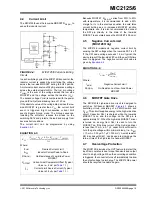
Page 16: ...e of the buck converter The SW pin also senses the current by monitoring the voltage across the low side MOSFET during OFF time In order to sense the current accurately connect the low side MOSFET dra...

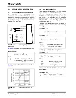
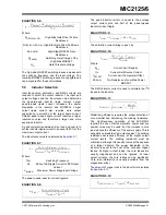
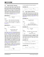
Page 17: ...OFF time period determined by the feedback voltage is less than the minimum OFF time tOFF min which is about 220 ns the MIC2125 6 control logic applies the tOFF min instead tOFF min is required to ma...

Page 18: ...g comparator ZC detection that monitors the inductor current by sensing the voltage drop across the low side MOSFET during its ON time If the VFB 0 6V and the inductor current goes slightly negative t...

Page 19: ...ng the SW voltage when the low side FET is off If the SW node voltage exceeds 12 mV typical the device turns off the low side FET until the next ON time event is triggered The negative current limit v...

Page 20: ...ETs are essentially equal to the power stage input voltage VIN A safety factor of 30 should be added to the VIN MAX while selecting the voltage rating of the MOSFETs to account for voltage spikes due...

Page 21: ...l and minimizing the winding resistance The high frequency operation of the MIC2125 6 requires the use of ferrite materials Lower cost iron powder cores may be used but the increase in core loss reduc...

Page 22: ...ripple Refer to the Ripple Injection subsection for details The voltage rating of the capacitor should be twice the output voltage for a tantalum and 20 greater for aluminum electrolytic or OS CON Th...

Page 23: ...n the range of 10 k to 49 9 k and calculate R1 using Equation 5 23 EQUATION 5 23 5 8 Ripple Injection The VFB ripple required for proper operation of the MIC2125 6 gm amplifier and comparator is 20 mV...

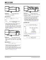
Page 24: ...SW via a resistor RINJ and a capacitor CINJ as shown in Figure 5 7 FIGURE 5 7 Invisible Ripple at FB The process of sizing the ripple injection resistor and capacitors is as follows Select CINJ as 10...

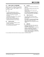
Page 25: ...o the switch node SW short Do not route any digital lines underneath or close to the inductor Keep the switch node SW away from the feedback FB pin The SW pin should be connected directly to the drain...

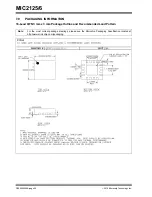
Page 26: ...Technology Inc 7 0 PACKAGING INFORMATION 16 Lead QFN 3 mm x 3 mm Package Outline and Recommended Land Pattern Note For the most current package drawings please see the Microchip Packaging Specificatio...

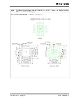
Page 27: ...2015 Microchip Technology Inc DS20005459B page 27 MIC2125 6 Note For the most current package drawings please see the Microchip Packaging Specification located at http www microchip com packaging...

Page 28: ...MIC2125 6 DS20005459B page 28 2015 Microchip Technology Inc...

Page 29: ...9 MIC2125 6 APPENDIX A REVISION HISTORY Revision A November 2015 Original Conversion of this Document Revision B December 2015 Corrected the erroneous listing of the MIC2126 example with a 64LD packag...

Page 30: ...MIC2125 6 DS20005459B page 30 2015 Microchip Technology Inc NOTES...

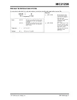
Page 31: ...ad 40 C to 125 C junction temperature range 16LD QFN b MIC2126YML 28V Synchronous Buck Controller featuring Adap tive On Time Control with Hyper Speed Control 40 C to 125 C junction temperature range...

Page 32: ...MIC2125 6 DS2005459B page 32 2015 Microchip Technology Inc NOTES...

Page 33: ...rademark of Microchip Technology Inc in other countries GestIC is a registered trademark of Microchip Technology Germany II GmbH Co KG a subsidiary of Microchip Technology Inc in other countries All o...

Page 34: ...86 24 2334 2829 Fax 86 24 2334 2393 China Shenzhen Tel 86 755 8864 2200 Fax 86 755 8203 1760 China Wuhan Tel 86 27 5980 5300 Fax 86 27 5980 5118 China Xian Tel 86 29 8833 7252 Fax 86 29 8833 7256 ASI...

Reviews: