

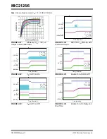


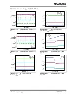
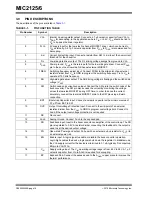


MIC2125/6
DS20005459B-page 24
2015 Microchip Technology Inc.
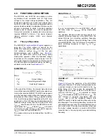
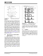
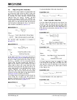
FIGURE 5-5:
Enough Ripple at FB.
The feedback voltage ripple is:
EQUATION 5-24:
• Inadequate ripple at the feedback voltage due to
the small ESR of the output capacitors.
The output voltage ripple is fed into the FB pin
through a feed-forward capacitor, C
ff
in this situation,
as shown in
. The typical C
ff
value is
between 1 nF and 100 nF.
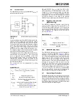
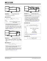
FIGURE 5-6:
Inadequate Ripple at FB.
With the feed-forward capacitor, the feedback
voltage ripple is very close to the output voltage
ripple.
EQUATION 5-25:
• Virtually no ripple at the FB pin voltage due to the
very low ESR of the output capacitors.
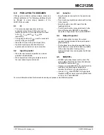
Therefore, additional ripple is injected into the FB pin
from the switching node SW via a resistor R
INJ
and a
capacitor C
INJ
, as shown in
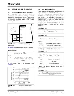
FIGURE 5-7:
Invisible Ripple at FB.
The process of sizing the ripple injection resistor and
capacitors is as follows.
• Select C
INJ
as 100 nF, which can be considered
as short for a wide range of the frequencies.
• Select C
ff
to feed all output ripples into the
feedback pin. Typical choice of C
ff
is 0.47 nF to
47 nF, if R1 and R2 are in the k
Ω
range. The C
ff
value can be calculated using
EQUATION 5-26:
• Select R
INJ
according to
.
EQUATION 5-27:
SW
FB
L
R1
R2
C
OUT
ESR
MIC2125/26
V
FB PP
R
2
R
1
R
2
+
--------------------
ESR
C
OUT
I
L PP
=
Where:
∆
I
L(PP)
Peak-to-Peak Value of the Inductor
Current Ripple
SW
FB
L
R1
R2
C
ff
C
OUT
ESR
MIC2125/26
V
FB PP
ESR
I
L PP
SW
FB
L
R
INJ
C
INJ
R1
R2
C
ff
C
OUT
ESR
MIC2125/26
C
ff
1
R
P
------
t
S
V
IN
D
1
D
–
V
IN
D
1
D
–
V
FB PP
–
------------------------------------------------------------------------------
»
Where:
V
IN
Power Stage Input Voltage
D
Duty Cycle
t
S
1/f
SW
R
P
(R1//R2//R
INJ
)
∆
V
FB(PP)
Feedback Ripple
R
INJ
1
C
ff
-------
V
IN
D
1
D
–
V
FB PP
f
SW
--------------------------------------------
=


