


2015 Microchip Technology Inc.
DS20005459B-page 19
MIC2125/6
4.4
Current Limit
The MIC2125/6 uses the low-side MOSFET R
DS(ON)
to
sense the inductor current.
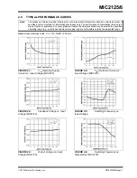
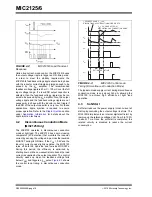
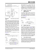
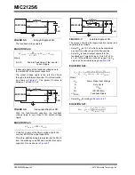
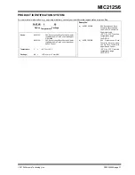
FIGURE 4-4:
MIC2125/6 Current-Limiting
Circuit
In each switching cycle of the MIC2125/6 converter, the
inductor current is sensed by monitoring the voltage
across the low-side MOSFET during the OFF period.
An internal current source of 36 µA generates a voltage
across the external resistor R
CL
. The I
LIM
pin voltage
V
(ILIM)
is the sum of the voltage across the low side
MOSFET and the voltage across the resistor (V
CL
).
The sensed voltage V
(ILIM)
is compared with the power
ground (P
GND
) after a blanking time of 150 ns.
If the absolute value of the voltage drop across the low
side MOSFET is greater than V
CL
, the current limit
event is triggered. Eight consecutive current limit
events triggers hiccup mode. The hiccup sequence,
including the soft-start, reduces the stress on the
switching FETs and protects the load and supply from
severe short conditions.
The current limit can be programmed by using
EQUATION 4-3:
Because MOSFET R
DS(ON)
varies from 30% to 40%
with temperature, it is recommended to add a 50%
margin to I
CL
in the previous equation to avoid false
current limiting due to increased MOSFET junction
temperature rise. It is also recommended to connect
the SW pin directly to the drain of the low-side
MOSFET to accurately sense the MOSFET’s R
DS(ON)
.
4.5
Negative Current Limit
(MIC2126 Only)
The MIC2126 implements negative current limit by
sensing the SW voltage when the low-side FET is off.
If the SW node voltage exceeds 12 mV typical, the
device turns off the low-side FET until the next ON-time
event is triggered. The negative current limit value is
given by
EQUATION 4-4:
4.6
MOSFET Gate Drive
The MIC2125/6 high-side drive circuit is designed to
switch an N-Channel MOSFET.
bootstrap circuit, consisting of a PMOS switch and
C
BST
. This circuit supplies energy to the high-side drive
circuit. Capacitor C
BST
is charged while the low-side
MOSFET is on and the voltage on the SW pin is
approximately 0V. When the high-side MOSFET driver
is turned on, energy from C
BST
is used to turn the
MOSFET on. If the bias current of the high-side driver
is less than 10 mA, a 0.1
μ
F capacitor is sufficient to
hold the gate voltage within minimal droop, (i.e.,
∆
BST
= 10 mA × 3.33
μ
s/0.1
μ
F = 333 mV). A small resistor,
RG in series with C
BST
, can be used to slow down the
turn-on time of the high-side N-channel MOSFET.
4.7
Overvoltage Protection
The MIC2125/6 includes the OVP feature to protect the
load from overshoots due to input transients and output
short to a high voltage. When the overvoltage condition
is triggered, the converter turns off immediately to allow
the output voltage to discharge. The MIC2125/6 power
should be recycled to enable it again.
R
CL
I
CLIM
PP
0.5
+
R
DS ON
V
OFFSET
–
I
CL
---------------------------------------------------------------------------------------------------------
=
Where:
I
CLIM
Desired Current Limit
∆
PP
Inductor Current Peak-to-Peak
R
DS(ON)
On-Resistance of Low-Side Power
MOSFET
V
OFFSET
Current-Limit Comparator Offset (Typical
Value is –4 mV per
I
CL
Current-Limit Source Current (Typical
Value is 36 µA, per
)
I
NLIM
12
mV
R
DS ON
--------------------
=
Where:
I
NLIM
Negative Current Limit
R
DS(ON)
On-Resistance of Low-Side Power
MOSFET


