


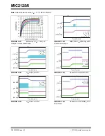


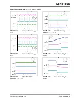
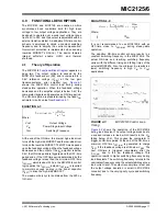

MIC2125/6
DS20005459B-page 4
2015 Microchip Technology Inc.
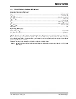
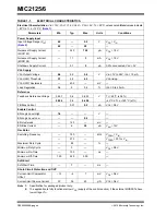
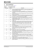
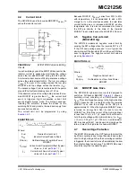
TABLE 1-1:
ELECTRICAL CHARACTERISTICS
Electrical Characteristics:
V
IN
= 12V, V
OUT
= 1.2V, V
BST
– V
SW
= 5V; T
A
= 25°C, unless noted.
Bold
values indicate
–40°C
≤
T
J
≤
+125°C.
(
.
Parameters
Min.
Typ.
Max.
Units
Conditions
Power Supply Input
Input Voltage Range (V
IN
)
(
4.5
—
5.5
V
V
DD
= V
IN
4.5
—
28
—
Quiescent Supply Current
(MIC2125)
—
340
750
µA
V
FB
= 1.5V
Quiescent Supply Current
(MIC2126)
—
1.1
3
mA
V
FB
= 1.5V
Shutdown Supply Current
—
0.1
5
µA
SW unconnected, V
EN
= 0V
V
DD
Supply
V
DD
Output Voltage
4.8
5.2
5.4
V
V
IN
= 7V to 28V, I
DD
= 10 mA
V
DD
UVLO Threshold
3.7
4.2
4.5
V
DD
rising
V
DD
UVLO Hysteresis
—
400
—
mV
—
Load Regulation
0.6
2
3.6
%
I
DD
= 0 to 40 mA
Reference
Feedback Reference Voltage
0.597
0.6
0.603
V
T
J
= 25°C (±0.5%)
0.594
0.6
0.606
–40°C
≤
T
J
≤
+125°C (±1%)
FB Bias Current
—
0.01
0.5
µA
V
FB
= 0.6V
Enable Control
EN Logic Level High
1.6
—
—
V
—
EN Logic Level Low
—
—
0.6
—
EN Hysteresis
—
120
—
mV
—
EN Bias Current
—
6
30
µA
V
EN
= 12V
Oscillator
Switching Frequency
—
750
—
kHz
V
FREQ
= V
IN
—
375
—
V
FREQ
= 50% x V
IN
Maximum Duty Cycle
—
85
—
%
—
Minimum Duty Cycle
—
0
—
V
FB
> 0.6V
Minimum On-Time
—
100
—
ns
—
Minimum Off-Time
150
220
300
—
Soft-Start
Soft-Start Time
—
7
—
ms
—
Short-Circuit Protection and OVP
Current-Limit Comparator
Offset
–15
–4
7
mV
V
FB
= 0.6V
Current-Limit Source Current
32
36
40
µA
V
FB
= 0.6V
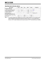
Note 1:
Specification for packaged product only.
2:
The application is fully functional at low V
DD
(supply of the control section) if the external MOSFETs have
low voltage V
TH
.