background image

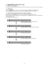
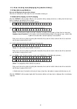
3.5.  Errors checking mode (Displaying the protection history)

3.5.1.Operation specifications

Error mode (Displaying the protection history):

When the set is started up in this mode, the error information is displayed.

3.5.2.About the display on the FL display

When the "

STATUS

" button is pressed after the error (protection history display) mode is set, a history like the one shown 

below is displayed, depending on the conditions.
(1)  Normal (when there has been no protection incident)

FLD

N O

P R O T E C T

(2)  For ASO (when the last protection incident was ASO protection)

FLD

P R T : A S O

Cause:

   The line between speaker terminals is shorted, or speakers with impedance of less than the rated value. 

Supplementary information:

   As the excess current is detected after operation of the speaker relay, a short on the 

speaker terminal and the connected speaker can be identified.

If the power is turned on without correcting the abnormality, the protection function will work about 5 seconds later 
and the power supply will be shut off.

(3)  For DC (when the last protection incident was DC protection)

FLD

P R T : D C

Cause:

  DC output of the power amplifier is abnormal. 

If the power is turned on without correcting the abnormality, the protection function will work about 5 seconds later 
and the power supply will be shut off.

(4)  For THERMAL (when the last protection incident was THERMAL(A) or THERMAL(B) protection)

FLD

P R T : T H E R M A L

A

FLD

P R T : T H E R M A L

B

Cause:

  The temperature of the heat sink is excessive. 

If the power is turned on without correcting the abnormality, the protection function will work about 5 seconds later 
and the power supply will be shut off.

b

  Additional causes of protection can be due to loose connections, associated components, Microprocessor, etc.

When the "

STATUS

" button is pressed again after the protection history as shown above is displayed, the normal display 

reappears.

43

Summary of Contents for NR1504 /U1B

Page 1: ...erating instructions without fail For purposes of improvement specifications and design are subject to change without notice AV Surround Receiver NR1504 U1B N1B N1SG K1B NR1504 S0678 1V03DM DG1305 Copyright 2013 D M Holdings Inc All rights reserved WARNING Violators will be prosecuted to the maximum extent possible Ver 3 Please refer to the MODIFICATION NOTICE ...

Page 2: ...ONE 50 PROCEDURE FOR UPGRADING THE VERSION OF THE FIRMWARE 50 1 How to update by DFW 50 2 How to update by DPMS 54 3 How to update by USB Memory 61 ADJUSTMENT 70 TROUBLE SHOOTING 75 1 POWER 75 2 Analog video 76 3 HDMI DVI 79 4 AUDIO 81 5 Network USB 84 6 SMPS 87 LEVEL DIAGRAM 89 BLOCK DIAGRAM 95 POWER DIAGRAM 96 WIRING DIAGRAM 97 PRINTED WIRING BOARDS 98 SCHEMATIC DIAGRAMS 1 25 107 HDMI_ADV3002 10...

Page 3: ...PHONE 31 40 2507844 FAX 31 40 2507860 KOREA D M SALES AND MARKETING KOREA LTD 2F YEON BLDG 88 5 BANPO DONG SEOCHO GU SEOUL KOREA PHONE 82 2 715 9041 FAX 82 2 715 9040 CANADA D M Canada Inc 5 505 APPLE CREEK BLVD MARKHAM ONTARIO L3R 5B1 CANADA PHONE 905 415 9292 FAX 905 475 4159 JAPAN D M BUILDING 2 1 NISSHIN CHO KAWASAKI KU KAWASAKI SHI KANAGAWA 210 8569 JAPAN D M Holdings Inc CHINA D M SALES AND ...

Page 4: ...an do with this manual Search for a Ref No phrase Ctrl Shift F You can use the search function in Acrobat Reader to search for a Ref No in schematic diagrams printed wiring board diagrams block diagrams and parts lists 1 Press Ctrl Shift F on the keyboard The Search window appears 2 Enter the Ref No you want to search for in the Search window and then click the Search button A list of search resul...

Page 5: ...g Adobe Reader 9 On the Document menu click Sign Magnify schematic printed wiring board diagrams 1 Ctrl Space mouse operation Press Ctrl Space on the keyboard and drag the mouse to select the area you want to view The selected area is magnified When you want to move the area shown hold down Space and drag the mouse When you want to show a full page view press Ctrl 0 on the keyboard Ctrl Space 0 Pr...

Page 6: ...een Example using Adobe Reader 9 On the Tools menu point to Select Zoom and then click Pan Zoom Window Magnify schematic printed wiring board diagrams 3 Loupe Tool function The Loupe Tool function lets you magnify a specific part of a diagram in a separate window Example using Adobe Reader X On the View menu point to Zoom and then click Loupe Tool The Loupe Tool window appears on the screen Exampl...

Page 7: ...tant safety parts that are indicated by the z mark on schematic diagrams and parts lists be sure to use the designated parts Be sure to mount parts and arrange the wires as they were originally placed For safety seasons some parts use tapes tubes or other insulating materials and some parts are mounted away from the surface of printed circuit boards Care is also taken with the positions of the wir...

Page 8: ...er effective number 2 digit effective number 1 2ohm 1 R 2 2 digit effective number decimal point indicated by R 1 digit effective number Units ohm Capacitors CE Aluminum foil electrolytic CA Aluminium solid electrolytic CS Tantalum electrolytic CQ Film CK Ceramic CC Ceramic CP Oil CM Mica CF Metallized CH Metallized HS High stability type BP Non polar type HR Ripple resistant type DL For change an...

Page 9: ...Personal notes 9 ...

Page 10: ... p 75 Ω ohms PR CR signal 0 7 Vp p 75 Ω ohms Frequency response 5 Hz 60 MHz 0 3 dB n n Tuner section Note μV at 75 Ω ohms 0 dBf 1 x 10 15 W Receiving Range FM 87 5 MHz 107 9 MHz AM 520 kHz 1710 kHz Usable Sensitivity FM 1 2 μV 12 8 dBf AM 18 μV 50 dB Quieting Sensitivity MONO 2 8 μV 20 2 dBf S N MONO 70 dB IHF A weighted DIRECT mode STEREO 67 dB IHF A weighted DIRECT mode Total harmonic Distortion...

Page 11: ...ble kit Please order it from Marantz Official Service Distributor in your region if necessary 8U 110084S EXTENSION UNIT KIT 1 Set 8U 110136S EXTENSION UNIT KIT 1 Set Refer to 48 page When you update the firmware by DFW you can use the following JIG RS232C to internal connector conversion adapter with 4P FFC cable kit Please order it from Marantz Official Service Distributor in your region if neces...

Page 12: ...PCB FRONT_CNT Ref No of EXPLODED VIEW 43 PCB SIDE_CNT Ref No of EXPLODED VIEW 46 PCB AUDIO_VIDEO ASSY Ref No of EXPLODED VIEW 45 TOP COVER PCB RC5_MX Refer to DISASSEMBLY 4 PCB RC5_MX and EXPLODED VIEW PCB RC5_MX Ref No of EXPLODED VIEW 48 POWER TRANS MAIN Refer to DISASSEMBLY 6 POWER TRANS MAIN and EXPLODED VIEW POWER TRANS MAIN Ref No of EXPLODED VIEW 31 PCB SMPS Refer to DISASSEMBLY 8 PCB SMPS ...

Page 13: ... diagram below about the shooting direction of each photograph Photographs with no shooting direction indicated were taken from the top of the set 1 FRONT PANEL ASSY Proceeding TOP COVER FRONT PANEL ASSY 1 Remove the screws The viewpoint of each photograph Shooting direction X View from the top Front side Shooting direction B Shooting direction D Shooting direction C Shooting direction A View from...

Page 14: ...screws 3 Remove the screws and Style pin Please refer to EXPLODED VIEW for the disassembly method of each PCB included in FRONT PANEL ASSY FFC N2801 CP4401 STYLE PIN Loosen Remove ACETA TAPE STYLE PIN Loosen Shooting direction D Shooting direction C STYLE PIN Loosen 14 ...

Page 15: ...2 RADIATOR ASSY Proceeding TOP COVER RADIATOR ASSY 1 Remove the screws 2 Remove the screws and Style pin View from the bottom Shooting direction D Shooting direction C STYLE PIN Loosen 15 ...

Page 16: ...e Style pin and screws 4 Disconnect the connector wires Please refer to EXPLODED VIEW for the disassembly method of each PCB included in RADIATOR ASSY FFC N2801 STYLE PIN Loosen Remove ACETA TAPE STYLE PIN Loosen STYLE PIN Loosen CP4801 CP4800 CP4802 16 ...

Page 17: ... COVER RADIATOR ASSY REG ASSY 1 Disconnect the connector wires then remove the screws Please refer to EXPLODED VIEW for the disassembly method of each PCB included in REG ASSY Shooting direction B CP4603 CP4602 CP4614 CP4615 17 ...

Page 18: ...4 PCB RC5_MX Proceeding TOP COVER PCB RC5_MX 1 Remove the screws 2 Disconnect the connector board Shooting of photograph A Board to board 18 ...

Page 19: ... PCB RC5_MX PCB HDMI ASSY 1 Disconnect the connector wires and FFC then disconnect the connector board NOTE When you remove a HDMI board be careful of breakage of PCB FRONT_CNT STYLE PIN Loosen cut FFC CX1000 N3405 N2801 Board to board 19 ...

Page 20: ... TOP COVER PCB RC5_MX PCB HDMI ASSY POWER TRANS MAIN 1 Cut the wire clamp band then disconnect the connector wires and Style pin 2 Disconnect the connector wires STYLE PIN Loosen CP4001 CP4142 Shooting direction B CP4603 CP4602 20 ...

Page 21: ... 3 Remove the Style pin 4 Remove the screws NOTE It will separate and TRANS will fall from SET if screws is removed Shooting direction D STYLE PIN Loosen CP4401 View from the bottom 21 ...

Page 22: ... connector wires then remove the screws Please refer to EXPLODED VIEW for the disassembly method of each PCB included in AV ASSY 8 PCB SMPS Proceeding TOP COVER PCB RC5_MX PCB HDMI ASSY PCB SMPS 1 Disconnect the connector wires then remove the screws CP4401 CP4401 CN4002 CP4142 22 ...

Page 23: ...Y AV ASSY PCB SMPS PCB SPK 1 Remove the screws 2 Disconnect the connector wires then remove the screws and Style pin View from the bottom STYLE PIN Loosen HOLDER Remove the screws after remove the RADIATOR ASSY CP4001 CP4801 CP4800 CP4802 CP4602 CP4603 23 ...

Page 24: ...e tuner frequency step to FM 50kHz 200kHz Change tuner frequency step to AM 10kHz 9kHz U model only 5 PANEL REMOTE LOCK Selection mode DISPLAY M DAX Selects to reject operations through panel buttons and the master volume knob on the main unit and operations via the remote control 6 Service Related Selection mode STATUS PRESET CH Selects the Diagnostic mode or Displaying the protection history mod...

Page 25: ...Error display q Model destination information w Firmware Package Version e Main μ com r Main 1st Boot Loader t DSP ROM y Audio PLD u GUI SFLASH i Ethernet DM860A 1st Boot Loader Hardware ID o Ethernet DM860A 2nd Boot Loader Rhapsody Flag Q0 Ethernet DM860A IMAGE Q1 Ethernet DM860A MAC ADDRESS information q Model destination information Model FLD NR1504 U model N R 1 5 0 4 U NR1504 N model N R 1 5 ...

Page 26: ...on FLD b d o Ethernet DM860A 2nd Boot Loader Rhapsody Flag FLD E t h e r n e t S B L Press the STATUS button FLD 0 A Q0 Ethernet DM860A IMAGE FLD E t h e r n e t I M G Press the STATUS button FLD Q1 Ethernet DM860A MAC ADDRESS information FLD E t h e r n e t M A C Press the STATUS button FLD 26 ...

Page 27: ... S P E R R O R 0 1 Please check DSP U1004 HDMI B D and around circuits Before DSP command is issued the DSP BUSY port does not change to L D S P E R R O R 0 2 When DSP data read is performed executing WRITE L does not result in ACK H D S P E R R O R 0 3 When DSP data read is performed executing REQ L does not result in ACK L D S P E R R O R 0 4 When DSP data writing is performed executing WRITE H ...

Page 28: ...he document GUI Image 8200 2593 2131 Firmware Version Mainμcom 0 0 2 3 0 0 1 6 Info display 5 2 0 0 3 2 6 1 6 0 8 5 DSP 8 2 0 2 A PLD 2 2 0 5 GUI 6 4 1 1 0 0 0 6 DM860 FBL 0 9 0 3 1 1 DM860 SBL B 2 0 1 2 0 9 2 1 0 5 4 6 DM860 IMG I 2 0 1 2 1 0 2 2 0 9 5 8 The 6th digit from the right for Main μcom The 5th digit from the right for Main μcom The 2nd digit from the right for Main μcom The 1st digit f...

Page 29: ...ach time you press the PRESET CH button the mode displayed on the FL DISPLAY changes While the desired mode name is displayed on the FL DISPLAY press the STATUS button The set is restarted and the selected mode takes effect The currently set item is marked with z q FLD F P V O L L O C K O n Operations using the main unit panel buttons and the master volume knob are rejected w FLD F P L O C K O n O...

Page 30: ... STATUS button to restart the set and make the setting take effect q FLD 1 S E R V I C E C H E C K This mode is used for confirming the Video and Audio signal paths Diagnostic mode The signal paths of the set can be easily confirmed after repair Refer to 3 4 DIAGNOSTIC MODE 31 page w FLD 2 P R O T E C T I O N The protection history can be checked Refer to 3 5 Errors checking mode 43 page e FLD 4 O...

Page 31: ...tem FL display settings Contents of confirmationRemarks 1 Analog Video signal Pass V 0 1 V I D E O P A S S Input Source CBL SAT CVBS input CVBS output b Input source can be switched 2 HDMI pass Main V 0 3 H D M I P A S S Input Source CBL SAT HDMI input HDMI output ETHERNET input HDMI output Front HDMI input HDMI output b Input source can be switched 3 HDMI CEC V 0 4 H D M I C E C Input Source CBL ...

Page 32: ...IGITAL fixed Sound mode MULTI CH STEREO Speaker Config all Speakers Small SW Yes Digital input Speaker output Digital input Preout output FRONT L R SW b Input source can be switched 3 HDMI A 0 5 H D M I Input Source CBL SAT Input Mode HDMI fixed Sound mode STEREO HDMI input Speaker output HDMI input Preout output FRONT L R b Input source can be switched 4 analog A D MAIN A 0 6 A D Input Source CBL...

Page 33: ...Y LAN8720 DM860A TC4051 OUT1 ADV8195 BUFFER SPI FLASH INPUT SELECT SLI11131 OSD TMDS SW ADV3002 ADV7623 HDMI TRANSCEIVER NR1504 VIDEO DIAGRAM Fig 1 Analog Video Signal Pass IN3 IN2 IN1 USB HDMI5 HDMI4 HDMI2 HDMI3 HDMI1 HDMI IN ETHERNET HDMI OUT FRONT HDMI CVBS IN CVBS MONITOR OUT BLOCK DIAGRAM 33 ...

Page 34: ... ETHERNET PHY LAN8720 DM860A TC4051 OUT1 ADV8195 BUFFER SPI FLASH INPUT SELECT SLI11131 OSD TMDS SW ADV3002 ADV7623 HDMI TRANSCEIVER NR1504 VIDEO DIAGRAM Fig 2 HDMI Pass Main IN3 IN2 IN1 USB HDMI5 HDMI4 HDMI2 HDMI3 HDMI1 HDMI IN ETHERNET HDMI OUT FRONT HDMI CVBS IN CVBS MONITOR OUT 34 ...

Page 35: ... ETHERNET PHY LAN8720 DM860A TC4051 OUT1 ADV8195 BUFFER SPI FLASH INPUT SELECT SLI11131 OSD TMDS SW ADV3002 ADV7623 HDMI TRANSCEIVER NR1504 VIDEO DIAGRAM Fig 3 HDMI CEC u COM IN3 IN2 IN1 USB HDMI5 HDMI4 HDMI2 HDMI3 HDMI1 HDMI IN ETHERNET HDMI OUT FRONT HDMI CVBS IN CVBS MONITOR OUT 35 ...

Page 36: ...FS DSP1INMCK R5F56108VNFP DM860SPDIF AUDIO PROCESSOR R2A15218FP INPUT SELECT VOLUME SDRAM Oscillation Amplifier PCM9211 DIR A D ARCSPDIF PCM1690 MAIN ZONE DAC DATAF DATAS DSP1INCSW DSP1INF EPM3032A AUDIO PLD DSP1IN64FS ETHERNET PHY LAN8720 HDMI RECEIVER PROCESSOR ADV 7623 HDMI TRANCEIVER MAIN OUT PORT MPIO_A SELECTOR ADSP21487 DIGITAL AUDIO DECODER 300MHz TUNER CONT IPOD POWER CONT MUTE RELAY FL C...

Page 37: ...INFS DSP1INMCK R5F56108VNFP DM860SPDIF AUDIO PROCESSOR R2A15218FP INPUT SELECT VOLUME SDRAM Oscillation Amplifier PCM9211 DIR A D ARCSPDIF PCM1690 MAIN ZONE DAC DATAF DATAS DSP1INCSW DSP1INF EPM3032A AUDIO PLD DSP1IN64FS ETHERNET PHY LAN8720 HDMI RECEIVER PROCESSOR ADV 7623 HDMI TRANCEIVER MAIN OUT PORT MPIO_A SELECTOR ADSP21487 DIGITAL AUDIO DECODER 300MHz TUNER CONT IPOD POWER CONT MUTE RELAY FL...

Page 38: ... ETHERNET PHY LAN8720 DM860A TC4051 OUT1 ADV8195 BUFFER SPI FLASH INPUT SELECT SLI11131 OSD u COM TMDS SW ADV3002 ADV7623 HDMI TRANSCEIVER NR1504 VIDEO DIAGRAM Fig 6 GUI menu IN3 IN2 IN1 USB HDMI5 HDMI4 HDMI2 HDMI3 HDMI1 HDMI IN ETHERNET HDMI OUT FRONT HDMI CVBS IN CVBS MONITOR OUT 38 ...

Page 39: ... Tone FLASH 12MHz SR TMDS NETWORK CONTROLLER DM860A MAIN MICOM 74VHCU04 FLASH MUX DATAC DSP1OUTFS DSP1INSB DSP1INS DSP1INFS DSP1INMCK R5F56108VNFP DM860SPDIF AUDIO PROCESSOR R2A15218FP INPUT SELECT VOLUME SDRAM Oscillation Amplifier PCM9211 DIR A D ARCSPDIF PCM1690 MAIN ZONE DAC DATAF DATAS DSP1INCSW DSP1INF EPM3032A AUDIO PLD DSP1IN64FS ETHERNET PHY LAN8720 HDMI RECEIVER PROCESSOR ADV 7623 HDMI T...

Page 40: ... FLASH 12MHz SR TMDS NETWORK CONTROLLER DM860A MAIN MICOM 74VHCU04 FLASH MUX DATAC DSP1OUTFS DSP1INSB DSP1INS DSP1INFS DSP1INMCK R5F56108VNFP DM860SPDIF AUDIO PROCESSOR R2A15218FP INPUT SELECT VOLUME SDRAM Oscillation Amplifier PCM9211 DIR A D ARCSPDIF PCM1690 MAIN ZONE DAC DATAF DATAS DSP1INCSW DSP1INF EPM3032A AUDIO PLD DSP1IN64FS ETHERNET PHY LAN8720 HDMI RECEIVER PROCESSOR ADV 7623 HDMI TRANCE...

Page 41: ...LASH 12MHz SR TMDS NETWORK CONTROLLER DM860A MAIN MICOM 74VHCU04 FLASH MUX DATAC DSP1OUTFS DSP1INSB DSP1INS DSP1INFS DSP1INMCK R5F56108VNFP DM860SPDIF AUDIO PROCESSOR R2A15218FP INPUT SELECT VOLUME SDRAM Oscillation Amplifier PCM9211 DIR A D ARCSPDIF PCM1690 MAIN ZONE DAC DATAF DATAS DSP1INCSW DSP1INF EPM3032A AUDIO PLD DSP1IN64FS ETHERNET PHY LAN8720 HDMI RECEIVER PROCESSOR ADV 7623 HDMI TRANCEIV...

Page 42: ...ne FLASH 12MHz SR TMDS NETWORK CONTROLLER DM860A MAIN MICOM 74VHCU04 FLASH MUX DATAC DSP1OUTFS DSP1INSB DSP1INS DSP1INFS DSP1INMCK R5F56108VNFP DM860SPDIF AUDIO PROCESSOR R2A15218FP INPUT SELECT VOLUME SDRAM Oscillation Amplifier PCM9211 DIR A D ARCSPDIF PCM1690 MAIN ZONE DAC DATAF DATAS DSP1INCSW DSP1INF EPM3032A AUDIO PLD DSP1IN64FS ETHERNET PHY LAN8720 HDMI RECEIVER PROCESSOR ADV 7623 HDMI TRAN...

Page 43: ...can be identified If the power is turned on without correcting the abnormality the protection function will work about 5 seconds later and the power supply will be shut off 3 For DC when the last protection incident was DC protection FLD P R T D C Cause DC output of the power amplifier is abnormal If the power is turned on without correcting the abnormality the protection function will work about ...

Page 44: ...e POWER LED red flashes as a warning according to the conditions in which the protection incident occurred 1 ASO DC PROTECTION Flashes at intervals of 0 5 seconds 0 25 seconds lit 0 25 seconds off 2 THERMAL A B PROTECTION Flashes at intervals of 2 seconds 1 second lit 1 second off 3 6 Operation Info mode 3 6 1 Specifications This mode displays the accumulated operating time power on count counts f...

Page 45: ...ime for 3 seconds or more 2 The FL Display indicates MEMORY SAVING while the Recovery is being performed FLD M E M O R Y S A V I N G 3 The FL Display indicates COMPLETE when the Backup is completed FLD C O M P L E T E Recovery 1 Hold down the PRESET CH and DISPLAY buttons at the same time for 3 seconds or more 2 The FL Display indicates MEMORY LOAD while the Backup is being performed FLD M E M O R...

Page 46: ...t e c t i o n P a s s This is displayed for 5 seconds before returning to the normal display 6 DM860A Reboot mode 6 1 Specifications When DM860A is hung up DM860A is restarted Even when Network standby is set Setup Menu Network IP Control Always ON DM860A can be reset 6 2 Operation 1 Turn on MAIN ZONE button and select NETWORK for the input source 2 Press and hold the DISPLAY and SOUND MODE button...

Page 47: ...hold DISPLAY and PRESET CH r When Initializing is displayed on FLD release the buttons If it is not displayed within 15 seconds try again from Step e t Wait until No Network Connection or Favorites is displayed on FLD y Press the Power operation X button to turn off and on the power q FLD N E T W O R K w FLD N o N e t w o r k C o n n e NETWORK not connected FLD F a v o r i t e s NETWORK connected ...

Page 48: ...ncorrect connection with in the JIG EXTENSION UNIT KIT may cause damage Connection of PCB HDMI JIG Preparation 8U 110084S EXTENSION UNIT KIT 1 Set 8U 110136S EXTENSION UNIT KIT 1 Set Insulation sheet Do not supply it 1 sheet Ground lead Do not supply it 1 pc Procedures 1 Remove the screws then remove the BACK PANEL 2 Disconnect the connector board Shooting of photograph A Board to board PCB HDMI 4...

Page 49: ... a ground lead or the like 4 Connect the six extension jig cables Connection table of Board to Board No Pin Ref No PCB Ref No PCB q 31 pin CP4604 SIDE CNT N3403 HDMI w 7 pin CP4605 SIDE CNT N3406 HDMI e 25 pin CP4606 FRONT CNT N34 07 HDMI r 13 pin CP4611 FRONT CNT N3404 HDMI t 7 pin CP4008 FRONT CNT N3402 HDMI PCB VIDEO Board to board Board to board Insulation sheet PCB HDMI PCB HDMI 1 3 4 5 2 49 ...

Page 50: ...he software D Flash ROM With software But you should write to the latest version of each region PROCEDURE FOR UPGRADING THE VERSION OF THE FIRMWARE NOTE When the following are replaced always rewrite with updated firmware using DFW Refer to parts list of HDMI PCB UNIT ASS Y PCB HDMI ASSY IC1023 R5F56108VNFP U1006 EN29LV160DBTI IC1012 EPM3032A TC44 IC1008 MX25L3206EM2I 12G U K MX25L6406EM2I 12G N U...

Page 51: ...ile simultaneously pushing the M DAX and SOUND MODE button of the front panel 2 Confirm the power indicator is green and WRITTING is displayed in the front panel 1 4 Run the DFW Run the DFW_0013_NR1504_ Rev X X X exe on desktop of PC 1 5 Communication check 1 Select the serial port number of RS 232C in PC 2 Click the Check Comm button 1 2 51 ...

Page 52: ...onnection of the AV receiver and PC refer to 1 2 Connection of the AV receiver b Check the operation mode of the AV receiver refer to 1 3 Turn on the AV receiver c Check the selection of the RS 232C port number of PC 1 6 Download the firmware 1 Click the Load button 2 Download the firmware from the specified download source to PC XXX XXXX XXX XXXX_WWWXXXXYYYY ZZZZ bin XXX XXXX_WWWXXXXYYYY ZZZZ bin...

Page 53: ... notice for firmware update a Keep the PC environment b Avoid the communication cable from the electrical noise source e g telephone cable AC line a fluorescent light c Don t remove cable during update d Don t turn off the power during update e Don t run other PC application during update f Stop the resident program on PC Virus checker and System check utility etc g Stop the screen saver on PC h S...

Page 54: ...s to select Start then press the ENTER button During update the power indicator lights in red and the GUI screen disappears And an approximately remaining time is indicated on the display When updating is complete the power indicator lights in green and normal status is resumed Cautions on Firmware Update In order to update the firmware you must have the correct system requirements and settings fo...

Page 55: ...ate in an environment that has little network load 08 Firmware file data of Main CPU was requested but error message was received C o n n e c t i o n F a i l 0 8 Check the network connection Carry out the update in an environment that has little network load 09 Firmware file data of Main CPU was requested but it timed out C o n n e c t i o n F a i l 0 9 Check the network connection Carry out the u...

Page 56: ...rk connection Carry out the update in an environment that has little network load 22 Log in to DPMS failed L o g i n f a i l e d 2 2 Reset and update again Carry out the update in an environment that has little network load 23 Line etc is busy when logging into DPMS S e r v e r i s b u s y 2 3 Carry out the update in an environment that has little network load 24 Connection to DPMS failed C o n n ...

Page 57: ...e update in an environment that has little network load 52 Connection to DPMS failed when firmware such as DSP and PLD was rewritten C o n n e c t i o n F a i l 5 2 Check the network connection Carry out the update in an environment that has little network load 54 Error message received regarding firmware data after the log in to DPMS when firmware such as DSP and PLD was rewritten U p d a t i n g...

Page 58: ...er Updating starts automatically 82 Receiving firmware for rewriting serial flash sent by DM860A failed when timed out U p d a t i n g f a i l 8 2 Turn off and on the power Updating starts automatically 83 Receiving firmware for rewriting serial flash sent by DM860A failed when an error U p d a t i n g f a i l 8 3 Turn off and on the power Updating starts automatically 84 Receiving firmware for re...

Page 59: ...ating starts automatically Carry out the update in an environment that has little network load AF Firmware download error message received line congestion when DM860A related firmware was rewritten Boot Loader Mode D o w n l o a d f a i l A F Turn off and on the power Updating starts automatically Carry out the update in an environment that has little network load B0 Firmware download error messag...

Page 60: ...m i n 50 52 54 58 5A 61 DSP D S P m i n 50 52 54 58 5A 61 GUI Serial Flash G U I m i n 50 52 54 58 5A 61 80 86 DM860A Boot Loader E S B L m i n A0 A4 A6 A7 AE B5 DM860A Image E I M G m i n A0 A4 A6 A7 AE B5 DM860A Image Emergency Mode U p d a t e r e t r y Confirming the firmware s number after upgraded After updating the firmware check the version Refer to 1 μcom DSP Version display mode 25 page ...

Page 61: ... not possible to use this unit by connecting the unit s USB port to a PC via a USB cable Do not use an extension cable when connecting a USB memory device 3 2 Unzip Download File Pleases unzip the downloaded file on PC s s copy to USBflash drive You can find firmwares folder after unzipped Please copy that folder to USB flash drive You have to put firmwares folder on root directly on USB flash drive ...

Page 62: ...4 K1 China E1C 100100190500 firmwares 100100190100 APLD bin DSP bin enc_update xml GUI bin IMG bcd MAIN bin SBL bcd 3 4 Insert the USB memory into a USB port NOTE Please UNPLUG LAN cable from the unit during update USB_AVR 4520E3_000100620100 0001 firmwares 000100620100 USB_NR1504U_100100190100 0001 firmwares 100100190100 Download firmware in USB flash drive 62 ...

Page 63: ... FL display shows the following message FL Display Upper F i r m U p d a t e Lower U p d a t i n g C o m p l e t e Cautions on Firmware Update Do not remove a USB memory until updating is completed Do not turn off the power until updating is completed Approximately 1 hour is required for the updating procedure to be completed Once updating starts normal operations on the this unit cannot be perfor...

Page 64: ...emory 0D Received value with invalid PackageVersion C o n n e c t i o n F a i l 0 D This unit automatically retries several times Wait until the FL display stops If the FL display stops at the Error display press and hold the ON STANDBY X button for five seconds 10 No UpdatePacket received from DM860A TimeOut U p d a t i n g f a i l 1 0 This unit automatically retries several times Wait until the ...

Page 65: ...splay stops If the FL display stops at the Error display press and hold the POWER button for five seconds 37 No FirmwareFile in USB F i l e s N o t F o u n d 3 7 This unit automatically retries several times Wait until the FL display stops If the FL display stops at the Error display press and hold the ON STANDBY X button for five seconds 38 FirmwareFile in USB for unsupported Model name area N o ...

Page 66: ...C o n n e c t i o n F a i l 5 A This unit automatically retries several times Wait until the FL display stops If the FL display stops at the Error display press and hold the ON STANDBY X button for five seconds 5B NACK received in response or no response from Sub for L command U p d a t i n g f a i l 5 B This unit automatically retries several times Wait until the FL display stops If the FL displa...

Page 67: ...econds 82 No UpdatePacket received from DM860A TimeOut U p d a t i n g f a i l 8 2 This unit automatically retries several times Wait until the FL display stops If the FL display stops at the Error display press and hold the ON STANDBY X button for five seconds 83 Abnormal data in UpdatePacket received from DM860A FormatError U p d a t i n g f a i l 8 3 This unit automatically retries several time...

Page 68: ...o w n l o a d f a i l B 1 This unit automatically retries several times Wait until the FL display stops If the FL display stops at the Error display press and hold the ON STANDBY X button for five seconds B2 Error notification received after rewriting DM860A Firm U p d a t i n g f a i l B 2 This unit automatically retries several times Wait until the FL display stops If the FL display stops at the...

Page 69: ...L D m i n 50 52 54 58 5A 64 DSP D S P m i n 50 52 54 58 5A 64 GUI Serial Flash G U I m i n 50 52 54 58 5A 62 64 80 86 DM860A Boot Loader E S B L m i n A0 A4 A6 A7 AE B5 DM860A Image E I M G m i n A0 A4 A6 A7 AE B5 DM860A Image Emergency Mode U p d a t e r e t r y Confirming the firmware s number after upgraded After updating the firmware check the version Refer to 1 μcom DSP Version display mode 2...

Page 70: ...t DC Voltmeter to test points FRONT Lch TP4800 FRONT Rch TP4802 CENTER ch TP4804 SURROUND Lch TP4804 SURROUND Rch TP4808 3 Connect the power cord to AC Line and set the power switch to ON 4 Presetting MASTER VOLUME counterclockwise c min SPEAKER Speaker terminal No load Do not connect speaker dummy resistor etc MODE MCH STEREO FUNCTION DVD 5 Within 2 minutes after the power on turn VR401 clockwise...

Page 71: ...s Mngmt z 2 Dynamic Comp z 3 Low Frequency z 4 DIRECT PURE DIRECT 2 channel z1 S D z5 S S DIRECT PURE DIRECT Multi channel z1 S D D D S S S STEREO S D S S S MULTI CH IN S D D D S S DOLBY PRO LOGIC g S D D D S S S DOLBY DIGITAL S D D D S S S DOLBY DIGITAL Plus S D D D S S S DOLBY TrueHD S D D D S S S S DTS NEO 6 S D D D S S S DTS SURROUND S D D D S S S DTS 96 24 S D D D S S S DTS HD S D D D S S S D...

Page 72: ... S DOLBY TrueHD S S S S DTS NEO 6 S S S S S S DTS SURROUND S S S S DTS 96 24 S S S S DTS HD S S S S DTS Express S S S S MULTI CH STEREO S S S S S VIRTUAL S S S S S z 1 During playback in PURE DIRECT mode the surround parameters are the same as in DIRECT mode z 6 This item cannot be set when Dynamic EQ is set to On z 7 For HD Audio whose sampling frequency of an input signal is more than 96 kHz thi...

Page 73: ... 1 channel DTS 96 24 DOLBY TrueHD DOLBY DIGITAL Plus DOLBY DIGITAL EX With Flag DOLBY DIGITAL EX With no Flag DOLBY DIGITAL 5 1 channel DOLBY DIGITAL 2 channel DTS SURROUND DTS HD MSTR F DTS HD HI RES F DTS SURROUND S S F DTS 96 24 F DTS EXPRESS F DTS NEO 6 CINEMA S S S DTS NEO 6 MUSIC S S S DOLBY SURROUND DOLBY TrueHD F DOLBY DIGITAL F DOLBY DIGITAL S F F DOLBY PRO LOGIC g MOVIE S S S DOLBY PRO L...

Page 74: ...arks is output A No video signal output S Superimposed on the picture indicated in A Only the picture in is output NOTE If you operate the menu while playing back 3D video content or computer s resolution e g VGA the playback video is replaced by the menu screen The playback video is not displayed behind the menu screen This unit does not show the status display while playing back 3D video content...

Page 75: ... defective parts Check 3 5 Errors checking mode Refer to 43 page Are there any incomplete connections in the connectors connecting between the various circuit boards Is a DC 5V voltage output when the cord supplying the power from the SMPS B D to the HDMI B D CX1000 is unplugged Check µ com periphery circuitry of HDMI B D and replace any defective parts Check circuitry and parts from CX1 on the HD...

Page 76: ...2 Analog video MONITOR OUT CVBS HDMI output NG Input CVBS SOURCE CBL SAT To A Input HDMI To troubleshooting 3 2 HDMI DVI 76 ...

Page 77: ...deo amplifier V IC5400 7pin Check power supply voltage of IC5400 and surrounding circuitry soldering The pattern between IC5400 and JK5400 are defective Is the signal output to selector IC5401 V 3pin Check power supply voltage of IC5401 and surrounding circuitry soldering Extend HDMI B D using a jig HDMI B D flaw Check connection of FRONT CONNECTOR BD and AV BD NO NO NO NO YES YES YES YES b Unless...

Page 78: ...73 R1269 R1267 U1006 MX29LV160DBTI R1252 R1253 C1350 R1304 R1300 R1299 R1250 R1259 R1251 R1246 C1103 R1258 R1257 R1248 R1309 C1345 C1343 R1249 R1255 R1254 R1245 C1341 C1360 C1358 R1280 R1279 C1376 C1372 R1284 R1311 R1283 R1282 R1281 R1244 C1048 C1083 C1055 C1043 TR1005 FB1010 C1021 C1033 C1009 R1021 R1024 TR1002 C1039 R1224 R1225 TR1009 R1023 C1093 TR1000 C1098 C1207 C1211 C1203 C1040 CP1001 C1091...

Page 79: ... s HDMI indicator lit If you use a non Marantz BD DVD player s proceed to YES 9 Is sound output from the set s speaker terminals when the TV s power is turned off or the connection cable between the TV and the set is disconnected There may be the a problem with the HDMI DVI cable Check connection Use a certified HDMI cable with the HDMI stamp Replace the HDMI DVI cable with one that is less than 5...

Page 80: ... resolutions of 1080P Use an HDCP compatible TV PC TVs cannot be used Check the TV s input setting referring to the TV s operating instructions The TV is defective If the TV is not compatible with resolutions of 1080P no picture will be output even if the BD DVD player s resolution is set to 1080P NO NO NO NO Please refer to the NR1504_HDMI Rx Tx Failure Detection Procedure Manual ver_1 00 of SDI ...

Page 81: ...gital or dts CHECK4 INPUT SURROND MODE SOURCE Audio output OK HDMI Don t care Legacy PCM2ch or DolbyDigital or dts CHECK6 INPUT Connect NR s connected in HDMI audio output OK HDMI This unit s HDMI OUT Other NR s HDMI IN Setting SURROND MODE SOURCE CEC STANDBY Don t care HBR audio DolbyTrueHD or dtsHD MA CHECK5 INPUT SURROND MODE SOURCE Audio output OK HDMI Don t care HBR audio DolbyTrueHD or dtsHD...

Page 82: ... zener diode and diode which are connected with the base of a power transistor short circuited MTZJ3 3B 1SS133 Is other transistor trouble Is other resistance trouble Turn on the power check that voltage of the section is normal and that idling electric current is flowing Replace the power transistor Replace the transistor Replace the resistance Replace the emitter resistance Replace the base resi...

Page 83: ...transmitted to AV B D CP5200 Once more check the connection of the connector When you can specify the troubled channel and function check the corresponding signal route The power supply of 7V is repaired The power amplifier is repaired Is the connector correctly connected with HDMI B D Connect the connectors properly The HDMI B D is repaired YES NO YES NO NO YES YES YES 83 ...

Page 84: ...ons due to the MAC address etc NO NO NO YES Is the LAN cable properly connected Turn off the power and check the LAN cable properly and then turn the power back on NO Checking the environment The U2802 and surrounding circuitry are defective Checking the set NR1504 YES YES YES YES Is output voltage 3 3V supplied from IC1000 Is output voltage 1 2V supplied from IC1006 Is the version of IMG or Ether...

Page 85: ... defective Is the wire properly connected between N2801 on the HDMI board and CN4401 on the USB board The U2806 and surrounding circuitry on the HDMI board are defective Connect the wire properly NO NO 5 2 USB device is not recognized U2602 and surrounding circuitry are defective Checking the set NR1504 If no picture is output Check the HDMI DVI circuit Are digital video signals BCLK VD0 VD7 outpu...

Page 86: ... R1547 R1074 R1070 R1078 Q1030 Q1006 R1082 R1549 JACK1004 R1079 R1075 R1071 Q1031 Q1007 R1083 R1551 Q1014 Q1013 IC1600 SLI11131AFCAY8H R1021 R1024 R1622 R1649 L1029 C1312 C1314 R1032 TR1004 TR1003 R1198 R1197 C1037 C1321 Q1033 C1036 TR1032 TR1006 C1322 R1028 R1031 R1029 U1000 ADV3002BSTZ R1027 TR1007 R1030 R1642 R1632 R1631 R1644 R1643 R1630 R1639 R1638 R1637 R1641 R1640 TR1002 IC1006 R1232 L1030 ...

Page 87: ...r short part of the PCB board Check the damage of each part Replace the damaged parts Replace the damaged parts Is the fuse F4140 blown Is there solder short circuit in the PCB board Is there a damaged part Replace the IC4140 TOP258MG and D4142 D4143 D4144 D4145 DC 5V is not output YES YES YES YES YES YES 6 SMPS 87 ...

Page 88: ...61 5600 6 3 NXA C4163 5600 6 3 NXA C4164 IC4143 KIA2431AP R4161 6K8 D C4166 100N K ZD4159 ZJ5 6B 1 2 4 3 ワ ワ L4140 SQ2014 BKT4141 D4145 1N4007 D4144 1N4007 D4143 1N4007 JP4140 JUMPER D4142 1N4007 C4142 DE2F3KY103MB3BM02 JP4141 JUMPER 0 01 250V C4148 ZD4158 ZJ39B R4150 1M R4148 2M2 TR4142 KTC3198G C4157 D4149 SRL3060P D4151 C4167 R4157 56 0 01 250V C4149 C4152 47 25 NXA R4153 6R8 R4149 2M2 C4155 10...

Page 89: ... 5 4 5dB MAX SIGNAL LEVEL DOLBY LIMIT LEVEL ALLch 3dBFS MASTER VOL 00dB時のGAIN設定 SW YES時 DIGITAL 2dB 2 0dB SW YES時 ANALOG 2dB 6 5dB 4 5dB SW NONE時 DIGITAL 2dB 12dB 10 0dB SW NONE時 ANALOG 2dB 12dB 6 5dB 16 5dB VOL 0dB 表示値 時の基本OFFSET SW NON時のOFFSET AD入力時のOFFSET 2 12 10 0dB 2 12 6 5 16 5dB 3dB SW NO 32dBFS DIG IN 38 5dBFS A D IN 20dBFS DIG IN 26 5dBFS A D IN LINE IN EXT IN H POUT SPEAKER DSP ANALOG R2...

Page 90: ...GRAM CENTER ch 2dB 0dBFS 10dBFS 20dBFS 30dBFS 40dBFS 20dBFS DIG IN PCM or DD Config1 26 5dBFS A D IN 200mV 30dB SP OUT 4 48Vrms 8Ω 29dB MAX SIGNAL LEVEL DOLBY LIMIT LEVEL ALLch 3dBFS 3dB 26 5dBFS DIG IN DD Config2 2 6 5 4 5dB EXT IN SPEAKER DSP R2A15218FP GAIN SR5008 ONLY PCM1690 D A PLD PRE OUT MUTE SR5008 ONLY 90 ...

Page 91: ...ch 2dB 0dBFS 10dBFS 20dBFS 30dBFS 40dBFS 200mV 30dB MAX SIGNAL LEVEL 9 5dB 2 20 6 12dB Config1 DOLBY LIMIT LEVEL ALLch 3dBFS 50dBFS 40dBFS DIG IN DD Config1 INPUT 30dBFS DD LFE PREOUT 317mVrms 34dBFS PCM IN 40 5dBFS A D IN INPUT 20dBFS DIG IN PCM 200mV A D IN EXT IN DSP R2A15218FP GAIN PRE OUT MUTE SR5008 ONLY PCM1690 D A PLD PRE OUT MUTE SW1 91 ...

Page 92: ...10dBFS 20dBFS 30dBFS 40dBFS 23dBFS DIG IN PCM or DD Config1 29dBFS A D IN 200mV 30dB SP OUT 4 48Vrms 8Ω 29dB 2 6 4dB MAX SIGNAL LEVE Config2 DOLBY LIMIT LEVEL 1 41Vrms ALLch 3dBFS 6dB 29 5dBFS DIG IN DD Config2 2 6 5 4 5dB EXT IN SPEAKER DSP R2A15218FP GAIN SR5006 ONLY PCM1690 D A PLD PRE OUT MUTE SR5008 ONLY PREOUT 150mVrms 92 ...

Page 93: ...8Ω 26dB 2 3 6 7dB NON CLICP MAX SIGNAL LEVEL 4 0Vrms Config2 DOLBY LIMIT LEVEL 1 41Vrms ALLch 3dBFS 3dB 26dBFS DIG IN DD EX Config1 2 3 1dB DOLBY LIMIT LEVEL 1 41Vrms ALLch 3dBFS SP OUT D A OUT 32 5dBFS DIG IN DD EX Config2 INPUT 23dBFS DIG IN D D 2 6 5 3 7 5dB INPUT 200mV A D IN Mch STEREO EXT IN SPEAKER DSP R2A15218FP GAIN SR5008 ONLY PCM1690 D A PLD PRE OUT MUTE SR5008 ONLY PREOUT 150mVrms 93 ...

Page 94: ... 30dB 40dB 10dB LINE IN 0dBFS 2 0Vrms PREOUT 18 0dB 0dBFS 10dBFS 20dBFS 30dBFS 40dBFS 20dBFS DIG IN PCM5100 200mV MAX SIGNAL LEVEL 2 00Vrms SPEAKER 30dB SP OUT D A from DA SB ch TO MAIN from F ch NET USB DAC R2A15218FP ZONE2 BD3812F LEVEL DIAGRAM ZONE2 16 0dB 94 ...

Page 95: ...30SC6MT PRE_FL_GND FRONT R GND SPK_RLY ADV7623 PRE_SL_GND A PLD DM860A PRE_C_GND PRE_SR_GND RC5 M X B D 40P SHIELD CARD CABLE D_GND V_GND SMPS_S3 MAIN SPK B D D10SB60 FRONT_CNT B D DIR PLATE FRONT HDMI AUDIO S2 VIDEO S4 A_GND VOL_IC AC CORD AMP B S1 H P MIC B D HDMI B D ADV3002 MAIN_CPU SIDE_CNT B D VIDEO INPUT B D TUNER PACK REG B D FRONT B D 5CH AMP B D SMPS B D NR1504 GND BLOCK DIAGRAM MAIN TRA...

Page 96: ...860A LAN8720A A3V56S30FTP 2 H27U1G8F2BTR MFI337S3959 M X 3 3V AC CORD MAIN TRANS S2 8V 8V S1 AMP B DM860A SLI11131 ADV7623 STBY 5V S5 VKK S4 VIDEO ADV7623 AD8195 ADV3002 MX25L6406EM21 12G CEC5V ADV3002 SWM5V TC74VHCT08AFT FL AC F2 FL AC F1 A TUNER 5 0V A 8 0V Pre A 8 0V Pre PCM9211 EPM3023A TC74VHCU04FT SN74LVC244APW ADSP21487KSWZ 2B DV5V HDMI_OUT STBY 3 3V MUTE3 3V M3 3V CPU SWM3 3V FLT D5V MX PO...

Page 97: ...E 40P CARD CABLE MAIN SPK B D H P MIC B D 8P WIRE H P D10SB60 23P CARD CABLE S2 TAP 40P AC CORD S3 TAP 5P WIRE P T SIDE CNT B D 10P WIRE B REG B D USB B D 5CH AMP B D 7808 SMPS B D MAIN POWER TRANS FRONT CNT B D FRONT HDMI B D RC5 M X B D NR1504 WIRING BLOCK DIAGRAM FRONT B D HDMI USB B D REG CNT B D VIDEO INPUT B D WIRING DIAGRAM 97 ...

Page 98: ...051 C1565 R1364 R1363 R1352 R1345 R1339 R1328 IC1018 NJM8080G R1378 R1361 IC1017 NJM8080G R1314 R1362 R1366 R1382 R1381 R1368 R1367 R1354 R1347 R1341 R1330 C1507 C2490 C1513 C1512 C1506 R1353 R1365 R1377 C2449 C2450 R1338 R1327 C1505 C1510C1504 R1319 R1313 C1496 R1344 C1521 R1375 R1351 R1320C1499 C1511 C1522 R1376 IN OP FI ADJ ICT C1471 C1482 R1315 R1316 C1497 N3404 C1077 N3405 Q1027 TR1024 R1425 ...

Page 99: ... C 1 2 4 7 C1231 C1544 TC74VHC08FT IC1021 R1444 R1482 R1513 R1518 C1553 R1036 R1446 R1473 R1475 R1503 R1542 R1544 C1479 C1483 R2509 R2511 C1494 C1495 C1519 C1520 IC1019 NJM8080G R1325 R1331 R1332 R1342 R1343 R1349 R1356 R1359 R1371 C1323 C2657 Q1001 R2814 R2816 TR1027 C1067 C2607 R2850 R2856 U2805 C1458 C1460 C1584 C1451 C1461 C1469 C1475 R1429 TR1025 C1485 C2602 C2603 C2614 C2621 C2623 C2631 C263...

Page 100: ... ZVOL_LATCH 22 SWM5V MX 14 TU_SDIO SDA 12 TU_RST ST 11 TU_GPIO2 TUNED 5 MVOL_DATA 6 MVOL_CLK 9 MX_R 7 MX_L 8 AGND 13 TU_SEN 10 AGND 15 TU_SCLK SCL 15P 20 DAGND 23P 15 DA_FL 14 DA_FR 16 DAGND 17 A D_R 18 DAGND 19 A D_L 21 DAGND 22 USB_R 23 USB_L 13P 19P 9 A 7V 15 D5V MX 7 M DGND 18 BT_LINK 6 A_ 7V 12 NC 19 TRG 15V 16 SWM5V MX 18 TRG GND 3 A_ 7V 4 A_ 7V 9 MVOL_CLK 10 MVOL_DATA 17 FRONT_IRIN 15 MUTE3...

Page 101: ...L_DATA 9 MVOL_CLK 8 M3 3V 17 FRONT_IRIN 15 MUTE3 3V 16 RC_IN 19 RC_OUT 20 KILLIR 13 NC 14 NC 6 A_ 7V 7 M DGND 5 A_ 7V 4 A_ 7V 3 A_ 7V 1 MICGND 3 DACRTGND 2 MIC_IN 2 DA 5V 1 DA 5V 17 TRG1 14 M3 3V 13 D GND 12 A 7V 23 DA_SBR 29 MICGND 21 DA_SBL 25 RETGND 24 RETGND 23 USB_L 6 MUTE_Z2 7 PRE_MUTE 14 DA_FR 9 DA_SL 6 DA_SBL 5 DA_SBR 8 DA_SR 7 DAGND 12 DA_C 11 DA_SW 13 DAGND 10 DAGND 19 A D_L 18 DAGND 16 ...

Page 102: ...247 R5297 R5294 R5298 R5275 R5269 R5270 C5241 R5308 R5301 R5307 C5250 IC5401 C5406 C 5 4 0 2 R5417 C5416 C5405 C5418 C5420 CN5201 IC5402 R5419 R5421 R5423 R5425 C5415 C5414 C5424 C5423 C5505 R5335 R5271 R5513 R5428 R5314 R5233 R5248 D5215 R5512 R5519 R5515 R5303 R5299 R5330 R5250 R5227 C5254 R5255 R5320 Q5214 Q5213 C5260 R5321 R5201 R5238 C5232 C5234 R5265 C 5 5 0 4 R 5 5 1 1 R5503 R5246 R 5 5 0 1...

Page 103: ...C4400 C4401 J4054 CLAMP Vkk GND Vkk OPEN FIL2 FIL1 OPEN OPEN CLAMP CLP4401 FRONT B D 6125FF500 R F500mAL CLP4400 CLAMP CLP4402 H PGND H PL H PDET MICGND H PR MIC 7V MICDET S BY_GRN_LED P DIRECTLED NC DOORDET KEY2 NC KEY3 ISELA ISELB VSELA VSELB D MGND KEY1 MICDET H PDET NC NC NC H PGND S BY_RED_LED H PL FRONT_IRIN SWM5V MZ POWERKEY H PR M DAX_LED FLCLK FLDATA FLCE1 FLRST A 7V M3 3V D MGND SWM3 3V ...

Page 104: ...D4811 C4827 R4885 R4877 R4876 R5028 ZD4816 J4895 D4828 R5033 R5036 R5035 R5052 C4823 C4821 J4878 Q4817 J4877 R5009 Q4816 VR4801 C4816 R5013 Q4843 R4851 R5012 Q4844 R5000 C4867 J4865 J4863 J4937 R4975 J4862 R4988 R5014 R5015 J4867 Q4846 C4871 J4930 J4938 J4864 R4990 J4936 J4889 R4858 J4873 R4844 J4872 J4931 J4880 R4854 ZD4803 R4860 R4843 R4850 J4868 R4852 J4875 J4858 J4866 J4876 R4846 R4849 R4845 Q...

Page 105: ...143 ZD4158 R4153 T1 6AL 250V REG_CNT_B D AGND AGND 8V_IN 8V_IN 8V_IN AGND AGND AGND 8V_IN BKT4602 9P MTG 5V_IN 5V_IN VGND VGND TRG GND TRG 15V TRG 15V 5V_IN 5V_IN 7028 07388 701 0 F4600 T1 6AL 250V AC_IN A_GND AC_IN AC_IN AC_IN VGND AC_IN F4602 F4603 T1 6AL 250V SCREW TIP T1 6AL 250V 9P F4601 F4604 T2 5AL 250V BURRING BKT4601 CN4600 D4616 R4605 D4617 C4614 J4604 J4605 J4610 D4612 D4618 D4615 D4620...

Page 106: ...N AGND AGND AGND AGND 8V_IN 5V_IN TRG GND TRG 15V TRG 15V 5V_IN 5V_IN 5V_IN VGND VGND Pb NJM2845DL1 RC 5 M X B D 7 RC_OUT 1 M_XR 12 A 7V 11 A 7V 10 A 7V 8 KILLIR 6 BT_LINK 5 FRONT IRIN 4 RC_IN 3 M_XL 9 A 7V 2 AGND 14 M3 3V 13 D MGND 18 TRG GND 19 TRG 15V 16 SWM5V MX 15 D5V MX 17 TRG1 UTC4580E IC4607 C4631 C4619 R4622 Q4601 C4629 C4623 R4620 Q4600 R4635 Q4604 Q4603 D4628 R4634 Q4605 R4619 R4623 R46...

Page 107: ...1193 RXC_C R1101 33 ADV3002_RST C1209 1N K C1211 1N K R1075 10K R1083 OPEN RT1N141C Q1005 RT1N141C Q1004 10K R1116 R1093 4K7 OPEN Q1012 1 2 3 4 5 6 7 8 9 10 11 12 71 72 73 74 75 76 77 78 79 80 49 50 51 52 53 54 55 56 57 58 59 60 61 62 63 64 65 66 67 68 69 70 31 32 33 34 35 36 37 38 39 40 41 42 43 44 45 46 47 48 13 14 15 16 17 18 19 20 21 22 23 24 25 26 27 28 29 30 U1000 ADV3002BSTZ INCDATA2 INCDAT...

Page 108: ... 2012 D_GND FHDMI_5V DDC_SDA HP_CTRLA 2 4 6 8 7 10 9 11 13 15 17 19 1 5 3 12 14 16 18 N1005 AD3PBJ19G0 REV_B Q1011 RT1N441C 1 2 4 6 8 10 12 11 14 13 15 17 19 30 29 27 25 23 21 16 18 20 39 40 37 38 36 34 32 7 5 3 9 35 33 31 24 26 28 22 41 AD8195 U1201 AD8195 IN0 IP0 IN1 IP1 VTTI IN2 IP2 IN3 IP3 AVCC ON0 OP0 VTTO ON1 OP1 AVCC ON2 OP2 ON3 OP3 COMP AVCC AVCC AVEE AVCC AVCC AVEE TX_EN PE_EN AVCC VREF_O...

Page 109: ...X_0 TX_0 DDCTX_SCL ZD1001 OPEN L1002 OPEN 2012 L1003 OPEN 2012 0 R1181 RXMCK RX64FS RXFS RXI2S1 RXI2S3 ARCSPDIF HIN_SELC HIN_SELA ADV7623_SPI_CS ADV7623_SPI_MI ADV7623_SPI_MO HSCL HSDA ADV7623_INT2 TXEN CEC_COM DATAS_ADV DATASB_ADV DSP1OUTFS_ADV DATAC_ADV R1552 0 Q1015 RT1N141C Q1017 RT1N141C R1110 4K7 R1113 4K7 RXD_1 RXD_2 DDCD_SCL R1108 47K 1K R1105 C1227 OPEN C1585 OPEN R1122 100 R1124 100 C123...

Page 110: ...L A3 3VL_PVDD2 DGND VD4 D16 DGND DGND VD5 D17 D1 2VL DGND C1630 100N K C1629 100N K NET1 2V E_RESETN VD7 VD6 VD4 VD1 VSYNC A3 3VL_PVDD1 DGND 470 F 1608 R1663 D3 3VL DGND D1 2VL HPG DGND NC34 D1 2VL DGND DGND DGND NC30 DGND DGND DGND DGND DGND NC20 NC24 A1 2VL A1 2VL D1 2VL D1 2VL DGND DGND NC12 NC16 DGND DGND DGND DGND DGND D1 2VL DGND DDCSDA D3 3VL A3 3VL D1 2VL DGND DGND MCUSCL RXB_1 RXB_2 100N ...

Page 111: ...1260 OPEN R1261 OPEN R1267 10 R1262 4K7 R1264 4K7 R1265 4K7 100N K C1350 C1349 100N K C1346 100N K C1344 100N K C1342 1N K R1257 33 C1340 1N K R1271 10K R1277 47 C1378 9P J 4 2 5 7 1 3 6 8 R1285 10K 4 AR C1382 100N K R1281 10K R1283 10K R1311 33 R1312 33 DSPD6 DSPD4 DSPD2 R1290 33 R1394 33 R1395 33 DSP1OUT64FS_ADV C1449 100N K 4 2 5 7 1 3 6 8 R1308 10K 4 AR 4 2 5 7 1 3 6 8 10K 4 AR R1307 R1306 OPE...

Page 112: ... R1238 100 R1236 100 R1235 100 OPEN 1608 R2231 R2230 0 C1306 100N K R1185 33 R1189 470 R1195 OPEN R1196 OPEN 10 16 MVG C2494 C2218 100N K 1608 4N7 J 2012 C2221 15P G C2212 C2219 100N K C2214 1N K R1211 33 DA3 3V R1210 33 R1208 OPEN 5 7 6 8 4 2 3 1 R1704 33 4 AR R2209 33 SBCK C1326 100N K C1325 100N K PLDAERR 256FSDIR1 AUDIO1 R1214 33 C1328 100N K C1336 100N K C1335 100N K RXI2S1 AP_CK AP_CS C1334 ...

Page 113: ...608 R1361 11K 1608 R1358 4K7 1608 R1357 OPEN 1608 DACRTNGND R1381 0 1608 DAGND DASR DASL DASW DAFR DA 5V 4K7 R2505 R2412 1K R2514 10K C2499 1U K 1608 C2498 1U K 1608 C2411 100N K C1456 1N K C1455 1N K R2512 10K R2509 10K C1476 1N K R1332 OPEN 1608 R1322 15K 1608 R1321 15K 1608 R1331 OPEN 1608 R1320 15K 1608 R1330 300K 1608 R1319 15K 1608 R1328 OPEN 1608 R1314 15K 1608 R1313 15K 1608 C1502 OPEN 160...

Page 114: ...0 4 7U K 1608 OPEN R2628 C2633 100N K C2635 100N K C2636 100N K C2638 100N K AV0DATA0 AV0DATA2 AV0_CTRL0 AV0_CTRL2 OPEN R2656 C2640 100N K C2641 1N K C2643 1N K AV1DATA0 AV1DATA2 R2630 33 10 R2632 C2646 OPEN 1608 C2645 4 7U K 1608 C2648 4 7U K 1608 C2650 470P K USBREXT C2653 1N K C2655 OPEN C2657 100N K OPEN R2639 C2674 OPEN C2669 OPEN C2671 OPEN C2673 OPEN 4K7 R2652 DM_A2 DM_A0 DM_A16 BA1 DM_A5 D...

Page 115: ...BD R2860 OPEN E_RESETN E_RESETN E_SPI_CS E_SPI_CS E_SPI_MIEO E_RXDMIEO E_SPI_REQ E_SPI_REQ E_SPI_MIEO E_RXDMIEO C2818 1N K 1608 USBD MIIRXD2 USBVBUSDRV USBVBUSDRV 4 7U K 1608 C2821 MIIPHYCLK MIITXD3 MIIMDC NET3 3V EV_SCL E_SPI_CS E_RESET E_SPI_MOEI ESDA ESDA ESCL R2830 49 9 F 1608 R2832 49 9 F 1608 C2822 OPEN 1608 R2817 100 33 R2815 33 R2814 33 R2813 C2813 470P K R2820 10K R2819 33 C2824 100N K EV...

Page 116: ...DSP_RST R1516 4K7 RXD_MI232O OPEN 1608 J1000 R1554 0 1608 OPEN 1608 C1541 C1544 OPEN 1608 C1543 4 7U K 1608 D1032 OPEN D3008 LRB521S 30 C1548 100N K H5V_DET TCK RXD_E20 KEY3 KEY1 THERMALB_DC_ASO DV_POWER MAIN_POWER TXEN R1458 OPEN R1457 33 R1454 33 DAC_RST M_DAX_LED E_SPI_CS R1449 33 R1451 33 JT_TDI JT_TDO R1464 OPEN R1462 OPEN R1481 33 DAC_MUTE R1509 33 R1508 33 E_TXDMOEI R1503 33 R1506 33 R1505 ...

Page 117: ...2 100K R1416 4K7 R1414 15K TR1023 2SC3052 C1534 10N K DCDET3 R1424 390 R1419 10K R1422 4K7 TR1024 2SC3052 R1421 OPEN R1420 120K R1423 470 R1425 4K7 Q1027 RT1N141C R1432 100 R1434 1K C1536 10N K TR1025 2SC3052 R1428 100 R1433 470 R1435 4K7 THERMALDETA SWM3 3V TR1026 2SC3052 R1438 OPEN R1437 OPEN DGND SWM3 3V DGND STBY5V SWM5V MX R1385 10K R1389 220K TR1017 2SD2114K R1391 3K3 C1528 100N K R1392 1K2 ...

Page 118: ...ICGND 2 4 6 1 3 5 7 C125Z2 07 N3406 9 11 13 15 17 19 21 23 25 2 4 6 8 10 1 3 5 7 16 12 14 22 18 20 24 N3407 C125Z2 25 1 3 5 7 9 11 33 35 37 39 12 14 16 18 20 22 24 26 28 30 32 17 15 13 19 21 27 25 23 31 29 4 2 8 6 10 34 36 38 40 1 0 15 40PB N3408 RC_IN WAKE_UP TU_SDIO SDA TU_GPIO2 TUNED TU_SCLK SCL NC NC NC NC NC NC NC NC NC NC NC NC NC D MGND VSELA ISELA KEY2 MICDET GRNLED M_DAX_LED FLDATA REDLED...

Page 119: ...C1083 OPEN C1085 OPEN C1092 OPEN C1094 OPEN C1097 OPEN R1026 10K 0 R1030 C1115 OPEN C1123 OPEN C1322 100N K C1039 100N K C1038 100N K C1129 OPEN C1133 OPEN C1136 OPEN C1139 OPEN C1142 OPEN C1147 OPEN C1153 OPEN C1159 OPEN OPEN C1079 2 1 4 3 IC1004 PST8448UR GND VDD CT VOUT OPEN C1096 D1036 LBAS16HT1G C1109 100N K 100N K C1113 47K R1043 C1120 OPEN C1130 100N K OPEN R1047 15P J 1608 C1025 C1091 470 ...

Page 120: ...7N M 50V R4012 10 2 C4003 47N M 50V L4003 SP 2507 C4011 47N M 50V C4002 47N M 50V R4010 10 2 L4002 SP 2507 R4002 10 2 C4009 47N M 50V 10 2 R4008 47N M 50V C4000 R4000 10 2 L4001 SP 2507 10 2 R4007 47N M 50V C4008 R4027 1K1 1 R4026 D4002 LBAS16HT1G Q4006 RT1N141C LBAS16HT1G D4004 LBAS16HT1G D4005 R4031 R4030 C4021 2N2 K C4022 2N2 K C4020 2N2 K C4017 2N2 K C4018 2N2 K C4057 100N R 250V 1 2 3 5 4 CN4...

Page 121: ...R A 7V A 7V M3 3V M3 3V SWM5V MX NC TRG GND NC MUTE3 3V FRONT_IRIN RC_OUT D5V MX ZVOL_LATCH ZVOL_DATA NC VOL_MUTE TU_SCLK SCL TU_GPIO2 TUNED DA_ 5V A_ 7V A_ 7V MVOL_DATA RL GND TU 5V AGND A 7V TRG GND TRG 15V NC AV 1 3 H1 NC NC TO HDMI RL B AGND A 7V DA_ 5V TRG GND AV 1 3 E1 RL B AGND A 7V M DGND A 7V PRE_MUTE DAGND DAGND DAGND A D_L USB_L A D_R DA_FL DA_FR DA_C DA_SW DA_FL DAGND DA_SL DA_SW DA_SL...

Page 122: ...V R5300 47 AMP_SBL AMP_SBR D5223 1N4007 AMP_SR PRE_SW AMP_SL 47 16 C5229 C5230 47 16 47 16 RA3 C5225 47 63 RA3 C5224 47 63 RA3 C5220 C5214 10N K 100 16 C5213 R5322 1K C5264 0 1 50 R5319 470K R5309 470K 22 50 C5246 C5249 22 50 10K R5296 R5274 470K R5291 470K A 7V R5243 OPEN C5268 22 50 R5321 100K INC2001AC1 Q5214 R5320 100K Q5213 OPEN INC2001AC1 Q5212 100K R5306 C5259 22 50 Q5211 OPEN 100K R5305 22...

Page 123: ...00 B 820 D R5400 COMP_SW2 CVBS_B JK5403_3 1 20 2 3 4 5 6 7 8 9 10 19 18 17 11 12 13 14 15 16 IC5402 NJM2586AVC3 Y1_IN Y2_IN Y3_IN Cb1_IN Cb2_IN PS Cb_OUT Y_OUT V2 Cr_OUT V2 Cr1_IN V1 Cr2_IN Cr3_IN Cb3_IN SW1 SW2 V1 GND C5405 10N K 10 11 12 13 14 15 16 5 4 3 2 1 6 9 8 7 IC5401 TC4051BFT VEE GND A B C VCC Y4 Y6 OUT Y7 Y5 INH Y0 Y3 Y2 Y1 100 10 C5421 JK5400_3 Y2 Y1 Cr L L L Y6 Y2 ON H NC NC V 5V V 5V...

Page 124: ...R5501 0 AGND TU_SEN TU_SCLK SCL C5508 100P J C5510 100P J C5512 100P J C5509 100P J R5518 OPEN R5502 1K R5520 OPEN C5500 OPEN R5516 0 R5512 1K R5519 0 R5515 OPEN R5505 OPEN R5500 0 R5506 82K R5504 82K 7 4 5 6 2 3 1 8 PACK5500 6 5 4 1 2 3 7 L5500 OPEN 6 5 4 1 2 3 7 L5501 OPEN TU_SDIO SDA TU_GPIO2 TUNED RST SDIO TU_5V TUNERL NR1604 NR1504 GPIO2 SEN SCLK TUNERR OPEN OPEN AV 1 3 A3 MODEL MODEL OPTION ...

Page 125: ...K ZD4402 ZJ15B ZD4401 ZJ22B F4400 6125FF500 R D4401 1N4007 R4427 150 P_DIRECTLED Q4404 RT1N141C M DAXLED R4432 R4430 220 Q4406 RT1N141C Q4408 RT1N141C R4460 0 R4435 100 R4437 100 C4428 1000N Z R4442 10 R4440 C4437 82P J C4435 100N K C4436 R4447 18K 3 2 4 1 AZ4580MTR IC4400 A MICDET C4444 100P J C4443 100P J C4439 100P J R4458 0 R4457 0 C4451 100N K D4412 LBAS16HT1G 2 1 3 VEC4400 R4426 150 LED4401 ...

Page 126: ...CP4800 1 2 3 5 4 CN4800 R4932 1K2 1 R4925 470K R4926 22K C_IN R4846 5K6 1 R4908 22K R4902 47K TR_THERMAL R4858 22K C4815 100N K R4814 22K R4805 56K DHPTHF1608 95T R4874 Q4825 KSA992F R4916 1K2 R4894 100K R4881 470K R4882 22K Q4816 KSA992F R4870 1K2 AGND R4841 1K2 1 R4834 470K R4835 22K R4801 100K R4922 3K3 1 R4928 220 C4839 220P 500V R4918 33K R4919 OPEN C4836 47 50 6 3 11 R4893 1K8 R4896 5K6 1 R4...

Page 127: ...5 OPEN R4964 OPEN C4896 47 50 6 3 11 R5083 OPEN 47 50 6 3 11 C4882 R5021 5K6 1 C4868 47 50 6 3 11 C4854 47 50 6 3 11 Q4833 OPEN R4937 5K6 1 R4987 22 1 C4874 OPEN R5076 0R47 2 Q4849 2SD2390 R5043 0R47 2 Q4840 2SD2390 Q4831 2SD2390 Q4836 2SB1560 1 3 2 TP4813 R4985 10K R4986 10K C4875 OPEN R5065 680K R5078 5K6 D4822 KDS160 R4989 270K R4952 10K Q4857 2N5401S Q4848 2N5401S Q4832 2N5551S HIGHR C4864 47 ...

Page 128: ... R4159 5K6 1 2 4 3 ワ ワ L4141 2 3 1 TR4140 KMB2D0N60SA 2 X 1 V 3 C 5 D 7 S 8 S 9 S 10 S 6 S IC4140 TOP258MG 1 2 3 5 4 CN4141 CNT 5P IC4142 PC123X2YFZ RLY4140 JZC 36FD 005 HLT T2AL AC INLET NEUTRAL LIVE 27mH L4140 T2AL F4140 50mH L4140 F4140 T3 15AL T1 6AL F4140 F4141 FB ONLY NR1604 N1B U1B MTZJ39B MTZJ16B OPEN MTZJ39B MTZJ39B OPEN OPTION 2M2 5 OPEN 2M2 5 OPTION 270K 0 01 56K 270K OPTION OPTION 100 ...

Page 129: ...608 RB721Q 40 IC4602 KIA7905PI C4617 OPEN OPEN C4614 C4615 OPEN 1 3 2 CP4603 5267 03A 1 3 5 7 9 4 6 8 2 CN4600 C125Z2 09 5 3 1 8 6 4 2 9 7 CP4601 C125Z1 09 5 3 1 8 6 4 2 9 7 CP4600 C125Z1 09 1 3 5 7 9 4 6 8 2 CN4601 C125Z2 09 4700 25 MHA C4608 C4609 4700 25 MHA IN OUT OUT OUT OUT IN IN TRG 15V TRG GND A 7V AGND TU 5V RL GND VIDEO_GND VIDEO 5V OUT IN IN 8V_IN AGND AGND AGND 8V_IN TRG GND TRG 15V 5V...

Page 130: ...GND COMPONENT SW2 V INA RLY_H P RLY_S C NC NC NC D MGND D MGND D MGND D MGND D MGND D MGND D MGND D MGND D MGND D MGND D MGND D MGND D MGND D MGND D MGND COMPONENT SW2 VAGND V 5V V 5V RLY_SB H P_GND RLY_F RLY_F H P_GND RLY_SB COMPONENT SW1 V INB D MGND AV 1 3 K1 TO AV B D VIDEO 5V VIDEO_GND VIDEO_GND REG_CNT 1 4 B2 VIDEO 5V TO HDMI AV 2 3 O7 NR1604 ONLY AV 2 3 O5 HDMI DIGITAL CNT D6 NR1604 ONLY HD...

Page 131: ...6 3 5 C4627 OPEN C4634 10 16 3 5 C4626 OPEN C4638 OPEN NJM2845DL1_33 IC4606 R4633 220 D4703 LBAS16HT1G Q4600 RT1P141C RT1P141C Q4605 2 5 3 1 4 NC OUT GND ON OFF IN IC4700 PQ120DNA1ZPH C4704 100N K R4639 OPEN C4644 100N K JP4602 0 JP4601 0 1 3 2 PJ 308 02 JACK4602 PJ 308 02 BK C4636 10 16 3 5 C4633 10 16 3 5 R4620 33K D4628 LBAS16HT1G C4628 OPEN RCA 206B 02 OR OR JACK4601 19 17 15 13 11 9 10 8 6 4 ...

Page 132: ...3 54 S5 15 S15 10 S6 1 S2 4 S1 18 S2 7 S12 4 S7 6 S13 6 S9 2 S4 4 S11 1 S8 2 S13 3 S2 1 S14 1 S2 1 S2 2 S2 6 S2 1 S3 1 S2 2 S2 1 S2 1 S2 1 S14 2 S2 1 S8 11 S2 1 S2 3 S8 2 S1 S1 S10 1 S2 2 TRANS NR1504 Marantz EXPLODE VIEW 6 2 1 3 9 8 5 4 7 EXPLODED VIEW WARNING Parts marked with this symbol z have critical characteristics Use ONLY replacement parts recommended by the manufacturer 132 ...

Page 133: ...h nsp is indicated on this table cannot be supplied When repairing the P W B ASS Y check the board parts table and order replacement parts z The parts listed below are for maintenance only might differ from the parts used in the unit in appearances or dimensions zPart indicated with the mark is not illustrated in the exploded view Personal notes 133 ...

Page 134: ...KING STYLE S E T TAPE CLEAR 21 18 NR1504 19 FB FB NR1504 19 FB NR1501 21 BOX BOTTOM TAPE O 1 SET FRONT SET FRONT 25 22 9 7 8 13 14 15 16 17 20 27 28 11 6 2 3 5 4 29 12 22 26 30 10 24 23 31 UK plug UK Only PACKING VIEW 134 ...

Page 135: ...refer to the last chapter zParts for which nsp is indicated on this table cannot be supplied z The parts listed below are for maintenance only might differ from the parts used in the unit in appearances or dimensions Personal notes 135 ...

Page 136: ...1 RXA_1 CGND RXA_0 RXA_0 TVDD RXA_C RXA_C CGND CVDD DDCA_SCL CVDD CGND RXC_C RXC_C TVDD RXC_0 RXC_0 CGND RXC_1 RXC_1 TVDD RXC_2 RXC_2 HP_CTRLD 5V_DETD DGND DVDD DDCD_SDA DDCD_SCL CVDD CGND RXD_C RXD_C TVDD RXD_0 RXD_0 CGND RXD_1 RXD_1 TVDD RXD_2 RXD_2 CVDD CGND TXPVDD Pin Function Descriptions Pin No Mnemonic Type Description 1 DDCC_SCL Digital input HDCP Slave Serial Clock Port C DDCC_SCL is a 3 ...

Page 137: ...ply This pin supplies power to the digital logic and I Os It should be filtered and as quiet as possible 37 TXPLVDD Power 1 8 V Power Supply 38 TXGND Ground TXPVDD Ground 39 TXPGND Ground TXPLVDD Ground 40 EXT_SWING Analog input This pin sets the internal reference currents Place an 887 Ω resistor 1 tolerance between this pin and ground 41 HPD_ARC Analog input Hot Plug Detect Signal This pin indic...

Page 138: ...ply This pin supplies power to the digital logic and I Os It should be filtered and as quiet as possible 37 TXPLVDD Power 1 8 V Power Supply 38 TXGND Ground TXPVDD Ground 39 TXPGND Ground TXPLVDD Ground 40 EXT_SWING Analog input This pin sets the internal reference currents Place an 887 Ω resistor 1 tolerance between this pin and ground 41 HPD_ARC Analog input Hot Plug Detect Signal This pin indic...

Page 139: ... 120 TVDD Power Receiver Terminator Supply Voltage 3 3 V 121 RXA_2 HDMI input Digital Input Channel 2 Complement of Port A in the HDMI Interface 122 RXA_2 HDMI input Digital Input Channel 2 True of Port A in the HDMI Interface 123 HP_CTRLB Digital output Hot Plug Detect for Port B 124 5V_DETB Digital input 5 V Detect Pin for Port B in the HDMI Interface 125 DGND Ground DVDD Ground 126 DVDD Power D...

Page 140: ...P5_OUT SCLK_OUT MCLK_OUT ARC RX EDID REPEATER CONTROLLER RX HPD CONTROLLER EP_MISO EP_MOSI EP_CS EP_SCK SPI MASTER SLAVE EQUALIZER RXB_0 RXB_1 RXB_2 EQUALIZER SAMPLER SAMPLER RXC_0 RXC_1 RXC_2 EQUALIZER SAMPLER RXD_0 RXD_1 RXD_2 EQUALIZER CEC CONTROLLER EDID RAM SAMPLER HDMI RECEIVER PROCESSOR TRANSMITTER PACKET BUILDER HDCP ENCRYPTION ENGINE HDMI ENCODER SERIALIZER TMDS DRIVERS INT1 INT2 INT_TX I...

Page 141: ...al audio data input 2 29 RXIN6 ALRCKI0 I Yes Biphase signal input 6 AUXIN0 LR clock input 2 30 RXIN5 ABCKI0 I Yes Biphase signal input 5 AUXIN0 bit clock input 2 31 RXIN4 ASCKI0 I Yes Biphase signal input 4 AUXIN0 system clock input 2 32 RXIN3 I Yes Biphase signal input 3 2 33 RXIN2 I Yes Biphase signal input 2 2 36 35 34 33 32 31 30 29 28 27 26 25 1 2 3 4 5 6 7 8 9 10 11 12 ERROR INT0 NPCM INT1 M...

Page 142: ... SELECTOR MPO 0 MPO 1 MAIN OUTPUT SCKO BCK LRCK DOUT PORT RXIN8 RXIN9 RXIN10 RXIN11 DITOUT AUTO DIR ADC AUXIN0 AUXIN1 AUXIN2 AUTO DIR ADC AUXIN0 AUXIN1 AUXIN2 AUTO DIR ADC AUXIN0 AUXIN1 DIT Lock DIR Unlock ADC AUXIN 2 AUXOUT OSC Divider XMCKO Divider XMCKO DITOUT RECOUT0 RECOUT1 AUXIN 0 AUXIN1 ADC Standalone ADC Mode Control Function Control REGISTER POWER SUPPLY MC SCL MDI SDA MDO ADR0 MS ADR1 FI...

Page 143: ... 106 DATA3 150 NC 19 NC 63 VDD_INT 107 TDO 151 ADDR8 20 NC 64 AMI_ACK 108 DATA4 152 ADDR9 21 VDD_INT 65 GND 109 VDD_EXT 153 CLK_CFG0 22 NC 66 THD_M 110 DATA5 154 VDD_INT 23 NC 67 THD_P 111 DATA6 155 CLKIN 24 VDD_INT 68 VDD_THD 112 VDD_INT 156 XTAL 25 NC 69 VDD_INT 113 DATA7 157 ADDR10 26 WDTRSTO 70 VDD_INT 114 TDI 158 SDA10 27 NC 71 MS1 115 SDCLK 159 VDD_EXT 28 VDD_EXT 72 VDD_INT 116 VDD_EXT 160 V...

Page 144: ...W9864G6JH 6 DIGITAL U1005 W9864G2IH Publication Release Date Aug 28 2009 4 Revision A03 4 PIN CONFIGURATION 144 ...

Page 145: ...L SIGNAL GENERATOR MODE REGISTER COLUMN DECODER SENSE AMPLIFIER CELL ARRAY BANK 2 COLUMN DECODER SENSE AMPLIFIER CELL ARRAY BANK 0 COLUMN DECODER SENSE AMPLIFIER CELL ARRAY BANK 3 DATA CONTROL CIRCUIT DQ BUFFER COLUMN DECODER SENSE AMPLIFIER CELL ARRAY BANK 1 NOTE The cell array configuration is 2048 256 32 ROW DECODER ROW DECODER ROW DECODER ROW DECODER A0 A9 BS0 BS1 CS RAS CAS WE 145 ...

Page 146: ...obe Command input When sampled at the rising edge of the clock RAS CAS and WE define the operation to be executed 18 CAS Column Address Strobe Referred to RAS 17 WE Write Enable Referred to RAS 16 28 59 71 DQM0 DQM3 Input Output Mask The output buffer is placed at Hi Z with latency of 2 when DQM is sampled high in read cycle In write cycle sampling DQM high will block the write operation with zero...

Page 147: ... 33 32 31 30 29 28 27 26 25 A16 BYTE Vss DQ15 A 1 DQ7 DQ14 DQ6 DQ13 DQ5 DQ12 DQ4 Vcc DQ11 DQ3 DQ10 DQ2 DQ9 DQ1 DQ8 DQ0 OE Vss CE A0 Standard TSOP Block Diagram WE CE OE State Control Command Register Erase V oltageGenerato r Input Output Buffers Program Voltage Generato r Chip Enable Output Enable Logic Data Latch Y Decoder X Decoder Y Gating Cell Matrix Timer Vcc Dete ctor A0 A19 Vcc Vss DQ0 DQ15...

Page 148: ...5 V VCOM 26 Voltage common decoupling AGND1 27 Analog ground 1 RSV2 28 Reserved tied to analog ground VOUT8 29 O No No Positive analog output from DAC8 VOUT8 30 O No No Negative analog output from DAC8 VOUT7 31 O No No Positive analog output from DAC7 VOUT7 32 O No No Negative analog output from DAC7 VOUT6 33 O No No Positive analog output from DAC6 VOUT6 34 O No No Negative analog output from DAC...

Page 149: ...VCC1 AGND1 VCC2 DAC VOUT7 VOUT7 DAC VOUT8 VOUT8 Digital Filter and Volume Power Supply and Common Voltage SCKI SCK Manager RST AMUTEO AMUTEI ZERO2 ZERO1 MODE MD SDA DEMP MC SCL FMT MS ADR0 RSV TEST ADR1 RSV Control Interface SPI I C HW 2 LRCK BCK DIN4 DIN3 DIN2 DIN1 Audio Interface PCM1690 SBAS448A OCTOBER 2008 REVISED JANUARY 2009 www ti com 8 Submit Documentation Feedback Copyright 2008 2009 Tex...

Page 150: ...41 AN1 IRQ9 B VREFL P40 AN0 IRQ8 B VREFH P05 TMO3 RxD4 IRQ13 A TCK PD7 D7 P97 AN15 AVCC PC4 A20 PC6 A22 RxD5 CS6 D PC7 A23 TxD5 CS4 D CS7 D P75 P76 IRQ14 A P77 P50 WR0 WR P51 WR1 BC1 P52 RD P53 BCLK P80 P81 TRSYNC VCC VSS P83 P54 TRDATA0 P55 TRDATA1 P56 TRDATA2 P57 WAIT TRDATA3 P84 P35 PO13 TIOCA1 TIOCB1 TCLKC A P36 PO14 TIOCA2 P37 PO15 TIOCA2 TIOCB2 TCLKD A P10 IRQ0 B P11 SCK2 IRQ1 B P12 RxD2 IRQ...

Page 151: ...N I I I I Remote control signal input pin 30 P27 PO7 TIOCA5 TIOCB5 SCK1 DAC MUTE O L L L DAC MUTE control pin PCM1690 31 P26 PO6 TIOCA5 TMO1 TxD1 RC OUT O H L H RC 5 CODE output pin 32 P25 PO5 TIOCA4 TMCI1 RxD1 KILL IR O L L L Front IR Disable control pin 33 P24 PO4 TIOCA4 TIOCB4 TMRI1 TU RST O SW3VPu L L L TUNER control 34 P23 PO3 TIOCC3 TIOCD3 E RESET O ODR N3VPu L L L ETHERNET RESET control pin...

Page 152: ...L L L TUNER GPIO2 input pin 68 P75 DSP ROMRST O I I I Memory reset for DSP Reset L 69 PC7 A23 CS4 D CS7 D TxD5 DSP MOSI O DA3VPu L L L DSP control pin ADSP21487KSWZ 3B 70 PC6 A22 CS6 D RxD5 DSP MISO I DA3VPu L L L DSP control pin ADSP21487KSWZ 3B 71 PC5 A21 CS5 D SCK5 DSPI CLK O DA3VPu L L L DSP control pin ADSP21487KSWZ 3B 72 PC4 A20 DSP RST O L L L DSP ADSP21487KSWZ 3B reset output pin Reset L 7...

Page 153: ...6 PE3 D11 ISEL B O L L L Input Selector rotation detection pin Rotary encoder 107 PE2 D10 VOL CLK O L L L FUNCTION VOLUME control pin R2A15218 108 PE1 D9 VOL DATA O L L L FUNCTION VOLUME control pin R2A15218 109 PE0 D8 PLD WRITE O L L L A PLD JTAG switching control pin 110 PD7 D7 JTAG TDO I L L L A PLD rewriting control pin JTAG 111 PD6 D6 JTAG TMS APLD CS O L L L A PLD rewriting control pin 112 P...

Page 154: ...DET ASO I I I I ASO PROTECT DC PROTECT HEAT PROTECT B detection pin 134 P46 IRQ14 B AN6 H P DET MIC DET THERMAL A I I I I MIC detection Headphone detection HEAT PROTECT A detection pin 135 P45 IRQ13 B AN5 KEY3 I SW3VPu I I I Button input 3 136 P44 IRQ12 B AN4 KEY2 I SW3VPu I I I Button input 2 137 P43 IRQ11 B AN3 KEY1 I SW3VPu I I I Button input 1 138 P42 IRQ10 B AN2 E SPI REQ I Pd I L I ETHERNET ...

Page 155: ...17 18 19 20 21 24 27 37 Exposed Pad 28 29 31 32 33 34 35 36 38 39 40 1 HS high speed LS low speed I input and O output NOTES 1 THE AD8195 LFCSP HAS AN EXPOSED PAD ON THE UNDERSIDE OF THE PACKAGE THAT AIDS IN HEAT DISSIPATION THE PAD MUST BE ELECTRICALLY CONNECTED TO THE AVEE SUPPLY PLANE IN ORDER TO MEET THERMAL SPECIFICATIONS AD8195 TOP VIEW Not to Scale 1 IN0 2 IP0 3 IN1 4 IP1 5 VTTI 6 IN2 7 IP2...

Page 156: ...ETB 37 IN_D_CLK 38 IN_D_CLK 39 I2C_ADDR1 40 I2C_SDA 80 P5V_A 79 P5V_B 78 P5V_C 77 P5V_D 76 DDC_SDA_A 75 DDC_SCL_A 74 DDC_SDA_B 73 DDC_SCL_B 72 DDC_SDA_C 71 DDC_SCL_C 70 DDC_SDA_D 69 DDC_SCL_D 68 DDC_SDA_COM 67 DDC_SCL_COM 66 CEC_IN 65 CEC_OUT 64 AMUXVCC 63 EDID_ENABLE 62 EDID_SDA 61 EDID_SCL PIN 1 INDICATOR ADV3002 TOP VIEW Not to Scale 60 IN_C_DATA2 59 IN_C_DATA2 58 HPD_C 57 IN_C_DATA1 56 IN_C_DA...

Page 157: ... X X X None X Don t care CS 1 2 3 4 8 7 6 5 SO SIO1 WP GND VCC HOLD SCLK SI SIO0 SYMBOL CS SI SIO0 SO SIO1 SCLK WP HOLD VCC GND Chip Select Serial Data Input for 1 x I O Serial Data Input Output for Dual Output mode Serial Data Output for 1 x I O Serial Data Output for Dual Output mode Clock Input Write protection 3 3V Power Supply Ground Hold to pause the device without deselecting the device DES...

Page 158: ...1 Vdd DQ0 VddQ NC DQ1 VssQ NC DQ2 VddQ NC DQ3 VssQ NC Vdd NC WE CAS RAS CS BA0 BA1 A10 AP A2 A3 Vdd A0 A1 DQM CKE Vss DQ15 VssQ DQ14 DQ13 VddQ DQ12 DQ11 VssQ DQ10 DQ9 VddQ DQ8 Vss NC DQMU CLK CKE A12 A11 A8 A7 A6 A5 A4 Vss A9 Vss DQ7 VssQ NC DQ6 VddQ NC DQ5 VssQ NC DQ4 VddQ NC Vss NC CLK A12 A11 A8 A7 A6 A5 A4 Vss A9 PIN CONFIGURATION TOP VIEW PIN CONFIGURATION TOP VIEW x8 x16 1 2 3 4 5 6 7 8 9 10...

Page 159: ...and address and data and to output data during read program operations The inputs are latched on the rising edge of Write Enable WE The I O buffer float to High Z when the device is deselected or the outputs are disabled CLE COMMAND LATCH ENABLE This input activates the latching of the IO inputs inside the Command Register on the Rising edge of Write Enable WE ALE ADDRESS LATCH ENABLE This input a...

Page 160: ...x 8 bit NAND Flash Figure 4 Block Diagram ADDRESS REGISTER COUNTER PROGRAM ERASE CONTROLLER HV GENERATION COMMAND INTERFACE LOGIC COMMAND REGISTER DATA REGISTER IO RE BUFFERS Y DECODER PAGE BUFFER X D E C O D E R 1024 Mbit 32 Mbit NAND Flash MEMORY ARRAY WP CE WE CLE ALE A27 A0 160 ...

Page 161: ...GND AGND SBRCIN SBLCIN AGND SBLC FR Pre OUT FL Pre OUT SBR Pre OUT TRER SUBR2 SUBL2 SRCIN SLCIN SR Pre OUT SL Pre OUT SBL Pre OUT INR12 INL12 INR13 INL13 INR14 INL14 CC AGND DGND REC ATT 0 6 12 18dB Bass Treble 14 14dB 2dB step 42 95dB 0 5dBstep 42 95dB 0 5dBstep 42 95dB 0 5dBstep 42 95dB 0 5dBstep 42 95dB 0 5dBstep 42 95dB 0 5dBstep Tone 42 0dB 0 5dBstep Tone Bass Treble 14 14dB 2dB step 0 95dB 0...

Page 162: ...2 FL DISPLAY FLD 018BT021GINK FRONT U4400 PIN CONNECTION GRID ASSIGNMENT 162 ...

Page 163: ...ANODE CONNECTION 163 ...

Page 164: ...3206Y0050S 1 ZD4800 963202500300D ZJ5 1A 0 5W 5MA 52MM SEMTECH K06005R134522S 1 ZD4801 4802 963202500280D ZJ3 3B 0 5W 5MA 52MM SEMTECH K06003R344522S 2 ZD4803 963202500300D ZJ5 1A 0 5W 5MA 52MM SEMTECH K06005R134522S 1 ZD4804 4805 963202500280D ZJ3 3B 0 5W 5MA 52MM SEMTECH K06003R344522S 2 ZD4806 963202500300D ZJ5 1A 0 5W 5MA 52MM SEMTECH K06005R134522S 1 ZD4807 4808 963202500280D ZJ3 3B 0 5W 5MA ...

Page 165: ... AX C00002236P520S 1 R4909 nsp 220K J 1 16W 1608REEL C20002246M160S 1 R4910 00D2412399954 2 7K J 1 5W 52RE AX C00002726P520S 1 R4911 nsp 10K J 1 16W 1608REEL C20001036M160S 1 R4912 4913 00D9630345903 RSD R1 2WJ 0 47 3 5 8 6 P 5MM SMALL R REEL N113136647820S 2 R4914 nsp 5 6K J 1 16W 1608REEL C20005626M160S 1 R4916 963121006340M 1 2K J 1 5W 52RE AX C00001226P520S 1 R4917 00D2412399954 2 7K J 1 5W 52...

Page 166: ...4574922 100UF M 50V 8 11 5 5RE SMS SY D040101087060S 1 C4825 nsp B470PF K 500V 5RE D00447127D050S 1 C4826 nsp X7R2200PF K 50V 2012REEL D011222777200S 1 C4828 4829 00D9630234302 10UF M 100V 6 3 11 5RE SMS SY D04010008C050S 2 C4830 4831 00D9630338402 330UF M 6 3V 6 3 11 5RE SMS SY D040331081050S 2 C4832 00D9630324607 47UF M 10V 5 11 5RE SMS SY Pb Free D040470082060S 1 C4835 nsp X7R0 1UF K 50V 1608RE...

Page 167: ...No Part Name Remarks Q ty New Ver TP4806 nsp 20010WR 03A00 DIP3P RIGHT ANGLE L101200100320S 1 TP4808 nsp 20010WR 03A00 DIP3P RIGHT ANGLE L101200100320S 1 VR4800 4804 963161012400S EVN DCAA03B13 REEL 1KB C541102315000S 5 4 ...

Page 168: ... 1 16W 1608REEL C20001016M160S 3 R4439 nsp 300 J 1 16W 1608REEL C20003016M160S 1 R4441 nsp 39K J 1 16W 1608REEL C20003936M160S 1 R4442 4443 nsp 10 J 1 16W 1608REEL C20001006M160S 2 R4444 nsp 0 J 1 16W 1608REEL C20000006M160S 1 R4445 nsp 47K J 1 16W 1608REEL C20004736M160S 1 R4446 nsp 100 J 1 16W 1608REEL C20001016M160S 1 R4447 nsp 18K J 1 16W 1608REEL C20001836M160S 1 R4449 nsp 820 J 1 16W 1608REE...

Page 169: ...55 4057 nsp 0 J 1 8W 3216REEL C200000061300S 3 J4059 4077 nsp JUMPER 0 6 52MM L045084006040S 19 JACK4400 963643006910M MINIJACK PJ 3234A 4 SILVER RINNG G401PJ323A40YS 1 JACK4401 963643101120S PHONE YUQIU D6 5 9P SILVER PJ 612A 9 G402PJ612A09YS 1 LED4400 963263012110S BL BUF4V5K 1 AV FP3 5 3PI RED 5MM REEL K500032000160S 1 LED4401 963209006790M BZ BB43V4V 2 FP5 TBF22A 5PI BLUE P 5MM K500056000130S ...

Page 170: ...1608REEL C20004716M160S 1 R5251 nsp 820K J 1 16W 1608REEL C20008246M160S 1 R5253 nsp 100 J 1 16W 1608REEL C20001016M160S 1 R5254 nsp 3 6K J 1 16W 1608REEL C20003626M160S 1 R5255 nsp 470K J 1 16W 1608REEL C20004746M160S 1 R5257 nsp 470K J 1 16W 1608REEL C20004746M160S 1 R5258 nsp 2 2K J 1 16W 1608REEL C20002226M160S 1 R5259 nsp 820K J 1 16W 1608REEL C20008246M160S 1 R5260 nsp 470 J 1 16W 1608REEL C...

Page 171: ...1 5RE SMS SY Pb Free D040R10087080S 1 C5246 5247 00D9630224503 22UF M 50V 5 11 5RE SMS SY D040220087060S 2 C5249 5250 00D9630224503 22UF M 50V 5 11 5RE SMS SY D040220087060S 2 C5252 nsp COG100PF J 50V 1608REEL D010101167160S 1 C5254 nsp X7R 0 01UF K 50V 1608REEL D010103777160S 1 C5274 nsp X7R 0 01UF K 50V 1608REEL D010103777160S 1 C5400 00D9630293709 100UF M 10V 5 11 5RE SMS SY D040101082070S 1 C5...

Page 172: ...SC 59 ISAHAYA J522101411210S 1 Q1022 1029 943216500020S RT1N141C 0 2W SC 59 ISAHAYA J522101411210S 8 Q1030 1031 943216500050S RT1N441C 0 2W SC 59 ISAHAYA J522104411210S 2 Q1033 943216500050S RT1N441C 0 2W SC 59 ISAHAYA J522104411210S 1 TR1000 1002 943216500050S RT1N441C 0 2W SC 59 ISAHAYA J522104411210S 3 TR1003 1004 963211500160D PBSS5140U SOT323 40V LOW VCEsat PNP TR J521051401010S 2 TR1005 9632...

Page 173: ...021M160S 1 R1135 1142 nsp 75 J 1 16W 1005REEL C20007506M101S 8 R1143 nsp 10K J 1 16W 1005REEL C20001036M111S 1 R1145 nsp 390K J 1 16W 1005REEL C20003946M101S 1 R1146 nsp 4 7K J 1 16W 1005REEL C20004726M101S 1 R1147 nsp 1K D 1 16W 1608REEL C20001021M160S 1 R1148 1149 nsp 33 J 1 16W 1005REEL C20003306M101S 2 R1150 nsp 10K J 1 16W 1005REEL C20001036M111S 1 R1154 nsp 4 7K J 1 16W 1005REEL C20004726M10...

Page 174: ...C20000006M160S 2 R1383 nsp 4 7K J 1 16W 1005REEL C20004726M101S 1 R1384 nsp 2 2M J 1 16W 1005REEL C20002256M101S 1 R1385 nsp 10K J 1 16W 1005REEL C20001036M111S 1 R1386 nsp 47K J 1 16W 1005REEL C20004736M101S 1 R1387 1388 nsp 100K J 1 16W 1005REEL C20001046M101S 2 R1389 nsp 220K J 1 16W 1005REEL C20002246M101S 1 R1390 nsp 27K J 1 16W 1005REEL C20002736M101S 1 R1391 nsp 3 3K J 1 16W 1005REEL C20003...

Page 175: ...C180103042100S 2 R2208 nsp 3 3K J 1 16W 1005REEL C20003326M101S 1 R2209 nsp 33 J 1 16W 1005REEL C20003306M101S 1 R2224 nsp 820 J 1 16W 1005REEL C20008216M101S 1 R2225 nsp 680 J 1 16W 1005REEL C20006816M101S 1 R2229 2230 nsp 0 J 1 16W 1005REEL C20000006M101S 2 R2232 nsp 0 J 1 16W 1608REEL C20000006M160S 1 R2235 nsp 33 J 1 16W 1005REEL C20003306M101S 1 R2252 2253 nsp 4 7K J 1 16W 1005REEL C20004726M...

Page 176: ...EEL D011104177101S 1 C1230 nsp X7R 0 01UF K 50V 1005REEL D011103777101S 1 C1231 1232 nsp X5R 10UF K 16V 2012REEL GRM21BR61C106KE15L D011106573200S 2 C1233 nsp X7R 0 01UF K 50V 1005REEL D011103777101S 1 C1234 nsp X7R 0 1UF K 16V 1005REEL D011104177101S 1 C1236 nsp X7R 0 1UF K 16V 1005REEL D011104177101S 1 C1237 nsp X7R 0 01UF K 50V 1005REEL D011103777101S 1 C1238 nsp X7R 0 1UF K 16V 1005REEL D01110...

Page 177: ...30 nsp X7R 1000PF K 50V 1005REEL D011102177101S 1 C1431 nsp X7R 0 1UF K 16V 1005REEL D011104177101S 1 C1432 1444 nsp X7R 1000PF K 50V 1005REEL D011102177101S 13 C1445 nsp X7R 0 1UF K 16V 1005REEL D011104177101S 1 C1446 nsp X7R 1000PF K 50V 1005REEL D011102177101S 1 C1447 nsp X7R 0 1UF K 16V 1005REEL D011104177101S 1 C1448 nsp X7R 1000PF K 50V 1005REEL D011102177101S 1 C1449 1451 nsp X7R 0 1UF K 16...

Page 178: ...D011475571160S 1 C2823 nsp X7R 4 7UF K 6 3V 1608REEL D011475571160S 1 C2824 2825 nsp X7R 0 1UF K 16V 1005REEL D011104177101S 2 C2845 nsp X7R 0 1UF K 16V 1005REEL D011104177101S 1 C2846 nsp X7R 1000PF K 50V 1005REEL D011102177101S 1 C2853 nsp X7R 0 1UF K 16V 1005REEL D011104177101S 1 OTHER PARTS GROUP CLP1001 nsp HMX9800 ON HAITAI W 2 6 L 50 WIRE SOLDER 4330000120000S 1 CP1001 nsp 1 0 16 23PB 2 23P...

Page 179: ...S 1 R4153 nsp 6 8 J 1 5W 52RE AX C0006R806P520S 1 R4154 nsp 10 J 1 16W 1608REEL C20001006M160S 1 R4155 nsp 10K J 1 16W 1608REEL C20001036M160S 1 R4156 nsp 4 7K J 1 16W 1608REEL C20004726M160S 1 R4157 nsp 56 J 1 5W 52RE AX C00005606P520S 1 R4158 nsp 3 3K J 1 5W 52RE AX C00003326P520S 1 R4159 nsp 5 6K J 1 5W 52RE AX C00005626P520S 1 R4160 nsp 22K F 1 16W 1608REEL C20002234M161S 1 R4161 00D2472041967...

Page 180: ...nsp PI5 2 REEL G645000050010S 1 F4600B nsp PI5 2 REEL G645000050010S 1 F4601 963652010500S T1 6A 250V IVBSUCPCcUR S506 N751501601160S 1 F4601A nsp PI5 2 REEL G645000050010S 1 F4601B nsp PI5 2 REEL G645000050010S 1 F4602 963652010500S T1 6A 250V IVBSUCPCcUR S506 N751501601160S 1 F4602A nsp PI5 2 REEL G645000050010S 1 F4602B nsp PI5 2 REEL G645000050010S 1 F4603 963652010500S T1 6A 250V IVBSUCPCcUR ...

Page 181: ...0S 1 C4056 00D9630244606 0 1UF M 50V 5 11 5RE SMS SY Pb Free D040R10087080S 1 C4057 nsp RED 0 1UF K 250V 5RE PCMT365 D02010407H080S 1 OTHER PARTS GROUP BKT4001 4002 nsp AVR1611BKE3 SECC t1 0 Sn plating PCB MTG 4010214876000S 2 BKT4005 nsp AVR133 HARMAN BURRING HOLE SPTE 0 8t SCREW 4010210196100S 1 CLP4001 nsp HMX9800 ON HAITAI W 2 6 L 50 WIRE SOLDER 4330000120000S 1 CLP4004 4005 nsp HMX9800 ON HAI...

Page 182: ...000S 1 20 Q422 00D9960018706 MAIN HEAT SINK TR 1 J5011560Y0000S 1 20 Q434 00D9960018706 MAIN HEAT SINK TR 1 J5011560Y0000S 1 20 Q446 00D9960018706 MAIN HEAT SINK TR 1 J5011560Y0000S 1 20 Q458 00D9960018706 MAIN HEAT SINK TR 1 J5011560Y0000S 1 21 Q409 963219003340S MAIN HEAT SINK TR 2 J502396400010S 1 21 Q421 963219003340S MAIN HEAT SINK TR 2 J502396400010S 1 21 Q433 963219003340S MAIN HEAT SINK TR...

Page 183: ...63B10S 3 S15 nsp SCREW 2S 3 8 ROUND BK BH B020230083B10S 10 nsp CM6001 F1B MARANTZ 2 75 6 5 0 45t 이붙이 TOOTHED 1530210126000S 1 nsp CABLE TIE DACT 100A 4330040343010S 5 nsp NR1403U1B MARANTZ NO_156 25 40 ACETATE 1220211449000S 1 nsp CM6001 F1B MARANTZ 2 75 6 5 0 45t 이붙이 TOOTHED 1530210126000S 2 963606502010M 1 0 40 280 A 4 4 8 8 0 035 0 65 AL 70MM N713402812480S 1 Ver 3 963606502030M 1 0 23 350 A 4...

Page 184: ...D MANUAL K K1 6517000001420S 1 18 963531103600M BOX GIFT 6007211420060S 1 19 nsp SHIPPING LABEL U1 5507000012980S 1 19 nsp SHIPPING LABEL N1BK 5507000012990S 1 19 nsp SHIPPING LABEL N1SG 5507000013000S 1 19 nsp SHIPPING LABEL K1 5507000013010S 1 20 nsp WARRANTY CARD U1 5727000000112S 1 20 nsp WARRANTY CARD K1 5727000000301S 1 21 nsp TAPE PACKING 1220210772000S 1 4 22 AAC LABEL 0 23 963544103490M S...

Reviews: