AD3V
P. 1 / 8 EM-1389 Rev.13
5-2-55, Minamitsumori, Nishinari-ku, Osaka 557-0063 JAPAN
Phone: +81(6)6659-8201 Fax: +81(6)6659-8510 E-mail: [email protected]
BEFORE USE ....
Thank you for choosing M-System. Before use, please check
contents of the package you received as outlined below.
If you have any problems or questions with the product,
please contact M-System's Sales Office or representatives.
■
PACKAGE INCLUDES:
Signal conditioner (body + base input resistor) ... (1)
Input resistor is provided only with current input type.
■
MODEL NO.
Check that model No. described on specification label is
exactly what you ordered.
■
INSTRUCTION MANUAL
This manual describes necessary points of caution when you
use this product, including installation, connection and basic
maintenance procedures.
POINTS OF CAUTION
■
CONFORMITY WITH EC DIRECTIVES
• This equipment is suitable for use in a Pollution Degree 2
environment and in Installation Category II, with the maxi-
mum operating voltage of 300V.
Basic insulation is maintained between the signal input and
output. Prior to installation, check that the insulation class
of this unit satisfies the system requirements.
• Altitude up to 2000 meters
• The equipment must be mounted inside a panel.
• Insert a noise filter for the power source connected to the
unit. TDK-Lambda Noise Filter Model MZS-1206-33 or
equivalent is recommended.
• The actual installation environments such as panel con-
figurations, connected devices, connected wires, may affect
the protection level of this unit when it is integrated in a
panel system. The user may have to review the CE require-
ments in regard to the whole system and employ additional
protective measures to ensure the CE conformity.
■
POWER INPUT RATINGS
• Operational range & power consumption: Check the power
rating for the unit on the specification label.
Rating 100 – 240V AC: 85 – 264V, 47 – 66 Hz, approx. 5VA
Rating 12 – 24V DC: 10.8 – 26.4V, approx. 4W
Rating 110V DC: 85 – 150V, approx. 4W
■
UNPLUGGING THE UNIT
Before you remove the unit from its base socket or mount it,
turn off the power supply and signal input for safety.
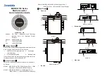
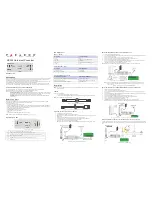
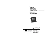
INSTRUCTION MANUAL
MODEL
AD3V
Input Resistor
A/D CONVERTER
(16-bit resolution)
Connection
Diagram Label
Base Socket
Body
Specification
Label
Clamp
(top & bottom)
DIN Rail
35mm wide
Spring Loaded
DIN Rail Adaptor
Shape and size of the base socket
are slightly different with various
socket types.
■
ENVIRONMENT
• Indoor use
• When heavy dust or metal particles are present in the air,
install the unit inside proper housing with sufficient ventila-
tion.
• Do not install the unit where it is subjected to continuous
vibration. Do not subject the unit to physical impact.
• Environmental temperature must be within -5 to +55
°
C (23
to 131
°
F) with relative humidity within 30 to 90% RH in order
to ensure adequate life span and operation.
■
WIRING
• Do not install cables (power supply, input and output) close
to noise sources (relay drive cable, high frequency line, etc.).
• Do not bind the unit's cables together with cables where
high noise levels are present. Do not install them in the same
duct.
■
AND ....
The unit is designed to function as soon as power is supplied,
however, a warm up for 10 minutes is required for satisfying
complete performance described in the data sheet.
COMPONENT IDENTIFICATION
INSTALLATION
Detach the yellow clamps located at the top and bottom of the
unit for separating the body from the base socket.
■
DIN RAIL MOUNTING
Set the base socket so that its
DIN rail adaptor is at the bot-
tom. Position the upper hook
at the rear side of base socket
on the DIN rail and push in the
lower. When removing the
socket, push down the DIN rail
adaptor utilizing a minus
screwdriver and pull.
■
WALL MOUNTING
Refer to the drawings in the
“TERMINAL CONNECTION”
section.