


LTC1760
43
1760fc
For more information
www.linear.com/LTC1760
A) Single Battery Configuration.
To limit the LTC1760 to a single battery, modify the
battery slot to be eliminated as follows:
1) Remove both FETs (Q5, Q6 or Q7, Q8) involved in
the discharge path.
2) Remove both FETS (Q3, Q4 or Q9, Q10) involved in
the charge path.
3) Remove the thermistor sensing resistors (R1A, R1B
or R2A, R2B).
4) Short the thermistor sense lines (TH1A, TH1B or
TH2A, TH2B) together at the IC.
5) Remove the diode (D2 or D3).
6) Unless otherwise specified, leave the unused pins
of the LTC1760 floating.
B) No Short-Circuit Protection Configuration.
1) Replace R
SC
with a short.
C) No LOPWR Protection.
1) Remove resistors R2 and R3 connected to LOPWR
and tie LOPWR to the V
CC
pin.
D) No DC Path Configuration.
To remove the DC input as part of the power path choices
to support the load:
1) Remove both FETs Q1 and Q2 involved in the DC
path.
2) Unless otherwise specified, leave the unused pins
of the LTC1760 floating.
E) No Charge Configuration.
To permanently disable the battery charger function:
1) Remove ALL FETs involved in the charge path (Q3,
Q4, Q9, Q10).
2) Remove switching FETs QTG, QBG, diode D1 and
inductor L1.
3) Remove diodes D2, D3, D4, capacitors C4, C
OUT
and
Resistor R11 and R
SENSE
.
4) Reduce C
IN
capacitor to 0.1µF.
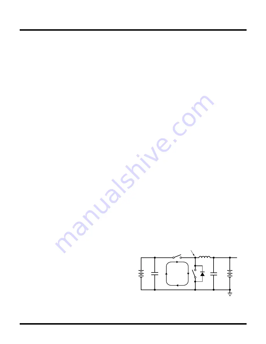
APPLICATIONS INFORMATION
1760 F10
V
BAT
L1
V
IN
HIGH
FREQUENCY
CIRCULATING
PATH
BAT
SWITCH NODE
C
IN
C
OUT
D1
Figure 11. High-Speed Switching Path
5) Remove all components connected to COMP1, V
SET
,
I
TH
, I
SET
, I
LIMIT
and V
LIMIT
pins.
6) Short I
LIMIT
and V
LIMIT
to GND.
7) Remove R1, C1 but short CLP to DCIN. Replace
R
CL
with a short/trace connection.
8) Short CSP to CSN but leave the combination floating.
9) Unless otherwise specified, leave the unused pins
of the LTC1760 floating.
F) No DC Path And No Charge Configuration.
To limit the LTC1760 to battery discharge functions
only, merge the previous two configurations with the
following:
1) Remove C
IN
.
2) Remove resistors tied to DCDIV. Ground DCDIV.
PCB Layout Considerations
For maximum efficiency, the switch node rise and fall times
should be minimized. To prevent magnetic and electrical
field radiation and high frequency resonant problems,
proper layout of the components connected to the IC is
essential. (See Figure 11.) Here is a PCB layout priority list
for proper layout. Layout the PCB using this specific order.
1. Input capacitors need to be placed as close as possible
to switching FET’s supply and ground connections.
Shortest copper trace connections possible. These
parts must be on the same layer of copper. Vias must
not be used to make this connection.


