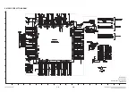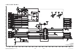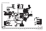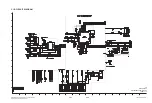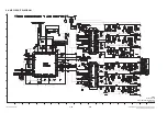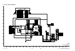
2-40
AIN1A
AIN1B
11
12
Stereo Analog Input 1
(Input) - The full-scale level is specified in the ADC Analog Characteristics
specification table.
AGND
13
Analog Ground
(Input) - Ground reference for the internal analog section.
VA
14
Analog Power
(Input) - Positive power for the internal analog section.
AFILTA
15
Antialias Filter Connection
(Output) - Antialias filter connection for the channel A ADC input.
AFILTB
16
Antialias Filter Connection
(Output) - Antialias filter connection for the channel B ADC input.
VQ
17
Quiescent Voltage
(Output) - Filter connection for the internal quiescent reference voltage.
TSTO
18
Test Pin
(Output) - This pin must be left unconnected.
FILT+
19
Positive Voltage Reference
(Output) - Positive reference voltage for the internal sampling circuits.
TSTO
20
Test Pin -
This pin must be left unconnected.
AIN4A/MICIN1
AIN4B/MICIN2
21
22
Stereo Analog Input 4 / Microphone Input 1 & 2
(Input) - The full-scale level is specified in the ADC
Analog Characteristics specification table.
AIN5A
AIN5B
23
24
Stereo Analog Input 5
(Input) - The full-scale level is specified in the ADC Analog Characteristics
specification table.
MICBIAS
25
Microphone Bias Supply
(Output) - Low-noise bias supply for external microphone. Electrical charac-
teristics are specified in the DC Electrical Characteristics specification table.
AIN6A
AIN6B
26
27
Stereo Analog Input 6
(Input) - The full-scale level is specified in the ADC Analog Characteristics
specification table.
PGAOUTA
PGAOUTB
28
29
PGA Analog Audio Output
(Output) - Either an analog output from the PGA block or high impedance.
VA
30
Analog Power
(Input) - Positive power for the internal analog section.
AGND
31
32
Analog Ground
(Input) - Ground reference for the internal analog section.
NC
33
34
No Connect
- These pins are not connected internally and should be tied to ground to minimize any
potential coupling effects.
TSTO
35
Test Pin
(Output) - This pin must be left unconnected.
VLS
36
Serial Audio Interface Power
(Input) - Determines the required signal level for the serial audio inter-
face. Refer to the Recommended Operating Conditions for appropriate voltages.
TSTI
37
Test Pin
(Input) - This pin must be connected to ground.
NC
38,
39,
40
No Connect
- These pins are not connected internally and should be tied to ground to minimize any
potential coupling effects.
SDOUT
41
Serial Audio Data Output
(Output) - Output for two’s complement serial audio data.
SCLK
42
Serial Clock
(Input/Output) - Serial clock for the serial audio interface.
LRCK
43
Left Right Clock
(Input/Output) - Determines which channel, Left or Right, is currently active on the
serial audio data line.
MCLK
44
Master Clock
(Input/Output) - Clock source for the ADC’s delta-sigma modulators.
DGND
45
Digital Ground
(Input) - Ground reference for the internal digital section.
VD
46
Digital Power
(Input) - Positive power for the internal digital section.
INT
47
Interrupt
(Output) - Indicates an interrupt condition has occurred.
OVFL
48
Overflow
(Output) - Indicates an ADC overflow condition is present.
Pin Name
#
Pin Description
SDA/CDOUT
1
Serial Control Data
(Input/Output) - SDA is a data I/O in IC
®
Mode. CDOUT is the output data line for
the control port interface in SPI
TM
Mode.
SCL/CCLK
2
Serial Control Port Clock
(Input) - Serial clock for the serial control port.
AD0/CS
3
Address Bit 0 (IC) / Co ntrol Port Chip Select (SPI)
(Input) - AD0 is a chip address pin in IC Mode;
CS is the chip-select signal for SPI format.
AD1/CDIN
4
Address Bit 1 (IC) / Ser ial Control Data Input (SPI)
(Input) - AD1 is a chip address pin in IC Mode;
CDIN is the input data line for the control port interface in SPI Mode.
VLC
5
Control Port Power
(Input) - Determines the required signal level for the control port interface. Refer
to the Recommended Operating Conditions for appropriate voltages.
RESET
6
Reset
(Input) - The device enters a low-power mode when this pin is driven low.
AIN3A
AIN3B
7
8
Stereo Analog Input 3
(Input) - The full-scale level is specified in the ADC Analog Characteristics
specification table.
AIN2A
AIN2B
9
10
Stereo Analog Input 2
(Input) - The full-scale level is specified in the ADC Analog Characteristics
specification table.
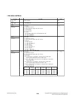
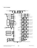
• PIN DESCRIPTION
Summary of Contents for SH33SD-S
Page 25: ...2 16 4 SLED CONTROL RELATED SIGNAL NO DISC CONDITION FIG 4 1 1 2 3 4 1 2 3 4 ...
Page 27: ...2 18 FIG 7 2 DVD 7 DISC TYPE JUDGEMENT WAVEFORMS FIG 7 1 DVD 1 2 3 IC501 IC501 1 2 3 1 2 3 ...
Page 28: ...2 19 FIG 7 4 CD FIG 7 3 CD 1 2 3 IC501 IC501 1 2 3 1 2 3 ...
Page 29: ...2 20 FIG 8 2 CD 8 FOCUS ON WAVEFORMS FIG 8 1 DVD 1 2 3 1 2 3 4 4 1 2 4 3 IC501 ...
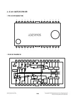
Page 41: ...2 32 2 IC401 MOTOR DRIVER PIN CONFIGURATION BLOCK DIAGRAM ...
Page 42: ...2 33 1 IC501 MPEG MT1389L PIN DESCRIPTION ...
Page 66: ...2 69 2 70 PRINTED CIRCUIT BOARD DIAGRAMS 1 MAIN P C BOARD DIAGRAM TOP VIEW ...
Page 67: ...2 71 2 72 MAIN P C BOARD DIAGRAM BOTTOM VIEW ...
Page 74: ...2 PASSIVE SUBWOOFER SH33SD W 950 A90 951 953 956 954 952 955 WIRE90 3 7 ...
Page 75: ......


