9. Calibration
- 102 -
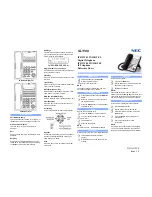
Figure 11-1 The top view of Test JIG
1. Test Jig Operation
1
2
3
4
ADI
TI-
- REMOTE
REMOTE
PS
VBAT
JTAG2
JTAG1
USB
TA
+
PS
_
POWER
ON
OFF
TA
POWER
MON
Status
UART
Status
ON
OFF
MON
UA
RT
PH
O
N
E
Power Source
Description
Power Supply
usually 4.0V
Travel Adaptor
Use TA, name is TA-20G(24pin)
Table 11-2 Jig Power
Switch Number
Name
Description
Switch 1
ADI-REMOTE
In ON state, phone is awaked. It is used ADI chipset.
Switch 2
TI-REMOTE
In ON state, phone is awaked. It is used TI chipset.
Switch 3
VBAT
Power is provided for phone from battery
Switch 4
PS
Power is provided for phone from Power supply
Table 11-3 Jig DIP Switch
Summary of Contents for MG810c
Page 1: ...Date May 2006 Issue 1 0 Service Manual MG810c MG810d Service Manual Model MG810c MG810d ...
Page 3: ... 2 ...
Page 5: ......
Page 46: ...4 TROUBLE SHOOTING 45 WR CS ADSSSSS CS ADSSSSS WR ...
Page 52: ...4 TROUBLE SHOOTING 51 G 1 Speaker Receiver Trouble Shooting Common Path ...
Page 53: ...4 TROUBLE SHOOTING 52 G 2 Speaker Receiver Trouble Shooting Acoustic Path ...
Page 54: ...4 TROUBLE SHOOTING 53 G 3 Speaker Receiver Trouble Shooting MP3 AAC Path ...
Page 55: ...4 TROUBLE SHOOTING 54 G 4 Speaker Receiver Trouble Shooting FM Radio Path ...
Page 56: ...4 TROUBLE SHOOTING 55 G 5 Main Mic Path Trouble Shooting ...
Page 57: ...4 TROUBLE SHOOTING 56 G 6 Ear Mic Receiver Path Trouble Shooting ...
Page 58: ...4 TROUBLE SHOOTING 57 G 7 Ear Mic Mic Path Trouble Shooting ...
Page 59: ...4 TROUBLE SHOOTING 58 G 8 Vibrator Trouble Shooting ...
Page 60: ...4 TROUBLE SHOOTING 59 4 2 RF Part Troubleshooting A RF Receiving Path Trouble Shooting ...
Page 64: ...4 TROUBLE SHOOTING 63 E RF Receiving Path Trouble Shooting FEM 1 ...
Page 65: ...4 TROUBLE SHOOTING 64 F RF Receiving Path Trouble Shooting FEM 2 ...
Page 67: ...4 TROUBLE SHOOTING 66 H RF Transmitter Path Trouble Shooting ...
Page 73: ...4 TROUBLE SHOOTING 72 N RF Transmitter Path Trouble Shooting FEM 1 ...
Page 74: ...4 TROUBLE SHOOTING 73 O RF Transmitter Path Trouble Shooting FEM 2 ...
Page 84: ...6 Block Diagram 83 6 Block Diagram ...
Page 85: ... 84 ...
Page 96: ... 95 8 PCB LAYOUT ...
Page 97: ... 96 8 PCB LAYOUT ...
Page 98: ... 97 8 PCB LAYOUT ...
Page 99: ... 98 8 PCB LAYOUT ...
Page 100: ... 99 8 PCB LAYOUT ...
Page 101: ... 100 8 PCB LAYOUT ...
Page 111: ... 110 ...
Page 113: ... 112 ...
Page 133: ...Note ...
Page 134: ...Note ...