background image

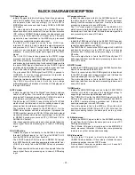
BLOCK DIAGRAM DESCRIPTION

- 31 -

1) RF/Analog mode:

- Initially the signal is fed to the Analog Tuner through antenna

cable via RF splitter. Now, here the Audio and Video signals
are separated and sent accordingly (i.e. audio SIF to
MSP4410sound processor and Analog CVBS to AN15865
AV Switch).

- The video signal is then passed to the VSP9437B colour

decoder and scan rate converter IC as per the user selection
(PiP or Main). VSP9437B chip decodes the video signal and
convert it into ITU-R 656 8bit Y/C signal while, The audio
signal which was transferred to the MSP chip is processed
there and converted into digital audio signal.

- The 656 8bit Y/C signal is now fed to the FLI2310 de-

interlacer IC which is used to make the signal progressive
and provides 4:2:2 16bit YC output while, The digital audio
signal is now transferred to the NSP6241 digital sound
processor. It converts the digital audio signal into the PWM
signal.

- The 16 bit YUV video is then passed to the PW181 image

processor and scalar IC. PW181 supports advanced scaling
and video processing techniques such as format conversion
and producing high quality video for advanced displays while
the audio PWM signal is transferred to the TAS5122 digital
amplifier which amplifies the level of audio signal and feed
them to the left and right speaker output accordingly.

- The processed 24bit RGB signal from PW181 is passed to

LGDP4410 IC. It is an image enhancement chip which is
used to improve the picture quality.

- Finally the improved quality 24bit RGB signal is transferred to

the LVDS chip which convert it into the low voltage
differential signal and interfaces it with the LCD display panel
through LVDS cable.

2) IDTV mode:

- Initially the signal is fed to the Digital Tuner through antenna

cable via RF splitter. It converts the signal into 8bit digital
data (called TS data) and pass it to the CI MAX chip which is
the hardware controller and PCMCIA card driver.

- The 8bit output of CI MAX IC is sent to the buffer 74LVC244

which stores the data and check the validity incase of pay
channels from the information through PCMCIA card.

- The final data is then passed to the STi5516B IC. It is the

MPEG video decoder and audio sub system. It produces the
CVBS signal(for main) and YUV(for PiP) and the audio signal
clocks and controls which are sent accordingly (i.e. audio I2S
to MSP4410 sound processor and DTV_CVBS and YUV to
AN15865 AV Switch).

- After these operations the audio and video signals follow the

same signal flow and processing as in case of RF/Analog
input.

3) AV-1/2/3 mode:

- Initially the signal is fed directly to the AN15865 AV switch

through 3 different inputs (I.e. AV-1 from full SCART, AV-2
from half SCART and AV-3 from front A/V).

- The SCART Audio(AV1,AV2) are fed to MSP4410K through

the LA7222 switch for selecting appropriate mode while Front
LR(AV3) is directly fed to the MSP4410K sound processor
IC.

- After these operations the audio and video signals follow the

same signal flow and processing as in case of RF/Analog
input.

4) Component mode:

- Initially the video signal is fed to the AN15865 switch IC and

the audio signal is sent to the MSP4410 sound processor
directly from the component input jack. From here the audio
processing is same as in case of RF mode.

- The YUV video signal is transferred to the X98014 ADC

which converts it into 24bit RGB and passes it to the FLI2310
de-interlacer IC and from there it follows the same signal flow
and processing as in case of RF mode.

5) DVI/DTV mode:

- Initially the TMDS signal is fed to the SiI 9021 TMDS receiver

chip which uses panel link digital technology to support high
resolution digital displays and HDTV.

- The TMDS Rxr IC converts the TMDS ssignal to 24 bit RGB

anddirectly transfers it to the PW181 scalar and image
processor and it follows the same processing as in case of
RF mode.

- The audio signal here is fed to the MSP directly from PC

audio input and from here the audio processing is same as in
case of RF mode.

6) DVI/PC mode:

- Initially the PC RGB signal is fed to the AN15865 switch from

where it is transferred to X98014 ADC

- There it is converted into 24bit RGB signal and is transferred

to the PW181 scalar and image processor and it follows the
same processing as in case of RF mode.

- The audio signal here is fed to the MSP directly from PC

audio input and from here the audio processing is same as in
case of RF mode.

7) HDMI mode:

- Initially the HDMI TMDS signal is fed to the SiI 9021 TMDS

receiver chip which uses panel link digital technology to
support high resolution digital displays and HDTV.

- The TMDS Rxr IC splits the HDMI TMDS signal into 24 bit

RGB and I2S audio signal It directly transfers 24bit RGB to
the PW181 scalar and image processor and it follows the
same processing as in case of RF mode.

- The audio signal is fed to the MSP via I2S switch which

switches between HDMI I2S and DTV I2S. After that the
audio processing follows the same path as in any other
mode.

8)  X-Studio mode:

- Initially the RGB/HV signal is fed to the AN15865 switching

IC and from there it follows the same path as in case of PC
RGB signal processing.

- The X-Studio LR signal is directly input to the MSP4410K

sound processor thereafter it follows the same processing
route as in any other mode audio processing.

9) S-Video mode:

- The S-video YC signal is directly transferred to the

VSP9437B video decoder IC from where it follows the same
processing path as in case of RF/TV mode.

- S-video doesn't have any separate audio port. It uses AV3

audio for sound output(front LR).

Summary of Contents for 37LP1DA-ZA

Page 1: ...TV SERVICE MANUAL CAUTION BEFORE SERVICING THE CHASSIS READ THE SAFETY PRECAUTIONS IN THIS MANUAL CHASSIS ML 03JA MODEL 37LP1DA ZA website http biz LGservice com e mail http www LGEservice com techsup html ...

Page 2: ...PRODUCT SAFETY 3 SPECIFICATION 6 TIMING CHART 11 ADJUSTMENT INSTRUCTION 12 SVC REMOCON 19 TROUBLE SHOOTING 20 BLOCK DIAGRAM 30 WIRING DIAGRAM 32 EXPLODED VIEW 33 EXPLODED VIEW PARTS LIST 34 REPLACEMENT PARTS LIST 35 SVC SHEET ...

Page 3: ...vely obtain and wear a commercially available discharging wrist strap device which should be removed to prevent potential shock reasons prior to applying power to the unit under test 2 After removing an electrical assembly equipped with ES devices place the assembly on a conductive surface such as aluminum foil to prevent electrostatic charge buildup or exposure of the assembly 3 Use only a ground...

Page 4: ...not shiny reheat them and if necessary apply additional solder Fuse and Conventional Resistor Removal Replacement 1 Clip each fuse or resistor lead at top of the circuit board hollow stake 2 Securely crimp the leads of replacement component around notch at stake top 3 Solder the connections CAUTION Maintain original spacing between the replaced component and adjacent components and the circuit boa...

Page 5: ...CIFICATION NOTE Specifications and others are subject to change without notice for improvement 3 General Specification No Item Specification Remark Min Typ Max Unit 1 Video Input applicable system 1 PAL SECAM BG EU Non EU PAL Market 2 PAL SECAM DK 3 PAL I 4 SECAM L L 5 NTSC M 6 PAL N M 6 7 South America Market 7 NTSC M 7 South America except other NTSC Market 2 AV input System 1 PAL 2 SECAM 3 NTSC...

Page 6: ...e Vrms Operating Current mA 14 Weight 21 5 22 5 23 5 kg TV Speaker 15 Size of Outline H 501 6mmX W 1051mmX D 109mm mm TV Speaker 16 SPEAKER Impedance 8 Tweeter 8 Regularity Output Power 15 15 W 17 Power On Time 9 Sec Stand by power on time 18 RS 232C 1 EA S W Download Half Scart 1 EA EU Full Scart 1 EA EU RF Input Analogue 1 EA UK 2 EA Non UK 2 TUNER DTV ID TV Only UK AV Input 1 EU Side 2 Non EU N...

Page 7: ... PFC power factor correction SMPS Table 1 RGB and DVI PC Input Mode Vertical Frequency Standard 0 5 Hz Vertical Lines Standard 7Lines No Resolution H freq KHz V freq Hz Pixel clock MHz Proposed Remark PC 1 720x400 31 469 70 08 28 32 DOS 2 720x400 37 927 85 03 35 50 DOS 3 640x480 31 469 59 94 25 17 VESA VGA 4 800x600 37 879 60 31 40 00 VESA SVGA 5 1024x768 48 363 60 00 65 00 VESA XGA 6 1280x768 47 ...

Page 8: ...75 8 Function Select AV control High 9 5 12V AV Mode Mid 5 8V Wide Screen 10 Low 0 2V TV Mode 9 Ground Green 10 Comms Data 2 11 Green input 0 7 V 75 12 Comms Data 1 13 Ground Red 14 Ground Blanking 15 Red input 0 7 V 75 16 RGB Switching Control High 1 3V RGB 75 Low 0 0 4V Composite 17 Ground Video input Output 18 Ground RGB Switching Control 19 Video output Composite 1V including sync 75 20 Video ...

Page 9: ... Ground blue 6 Audio input A left 0 5 Vrms 10 7 8 Function Select AV control High 9 5 12V AV Mode Mid 5 8V Wide Screen 10 Low 0 2V TV Mode 9 Ground Green 10 Comms Data 2 11 12 Comms Data 1 13 Ground Red 14 Ground Blanking 15 Red input 0 7 V 75 16 17 Ground Video input Output 18 19 Video output Composite 1V including sync 75 20 Video input Composite 1V including sync 75 21 Common ground Shield ...

Page 10: ...640 x 480 V Lines 85 008 509 480 1 3 25 6 H Pixels 40 0 37 879 1056 800 40 128 88 800 x 600 V Lines 60 317 628 600 1 4 23 7 H Pixels 49 5 46 875 1056 800 16 80 160 800 x 600 V Lines 75 0 625 600 1 3 21 8 H Pixels 56 25 53 674 1048 800 32 64 152 800 x 600 V Lines 85 061 631 600 1 3 27 9 H Pixels 57 283 49 725 1152 832 32 64 224 832 x 624 V Lines 74 55 667 624 1 3 39 10 H Pixels 65 0 48 363 1344 102...

Page 11: ... more than 15 minutes with signal maintained Connect input signal to the 24Pin DVI I Jack by using the D sub to DVI I Cable Select INPUT value as DVI PC Default value before adjustment Contrast shipment conditions Brightness shipment conditions Setting to PSM Standard 2 2 3 Operation status check 2 2 3 1 Operation mode Check designated mode accurately operates 2 2 3 2 Check of adjustment status an...

Page 12: ...DK BGIDKM BGIDKM BG I DK M Option1 1 Scart 1 0 SCART OFF 1 SCARTON 2 Sound Curve 0 0 Other area OFF 1 Middle Asia Vol ON 3 HDEV 0 0 HDEV OFF 1 HDEV ON No Item Condition Remark 4 OSD Lan 0 0 Eng Only 1 1 7 countries 7 countries in West Europe 2 11 countries West Europe Northern Europe 3 Farsi 4 Arab 5 Urdu6 English Hindi 7 East Asia4 8 English Tha 9 English China Option2 1 Download 0 0 Download dis...

Page 13: ...GB PC PW Version 3 00 Ucom Version 3 00 Input RGB PC PW Version 3 00 Ucom Version 3 00 If you press the menu button of remote control and the menu key of keypad till more 5 seconds simultaneously The service menu OSD will appear This service menu contain the RGB MSP NSP menus and 3 optional menus that is Option 0 1 2 If you want to correct the difference of colour gain of AD converter or set the P...

Page 14: ... Volume Nicam Prescale decides input signal level of Nicam audio signal Scart Prescale decides output signal level to speaker volume which is coming from SCART input IIS3 Prescale decides signal level of IIS3 signal line It decides output signal level to speaker volume which is coming from Digital sound input Scart1 Volume decides output level of Scart1 Full Scart2 Volume decides output level of S...

Page 15: ...etext If you want to see broadcasted text then you have to change Teletext data to 1 TOP If you want to use the Top option in Teletext you have to change Top data to 1 ACMS If you want to use the auto channel memory system for storing channels while auto programming you have to change ACMS data to 1 I IISave In Europe and Eastern Europe you have to change I II Save to 0 For other areas it is 1 A2 ...

Page 16: ... for updating the software the main Micom should not communicate with other Ics therefore to cut off the communication between main Micom and other Ics we set the value of Download to 1 SVC Cursor This setting disables or enables the working of navigation arrow keys while servicing the set The value is set to 0 for disable and 1 for enable RS232C This option is used while updating Scalar uControll...

Page 17: ...sh X STUDIO ISP Press to start ISP Input AV1 PW Version 2 09 Ucom Version 1 07 Input AV1 PW Version 2 09 Ucom Version 1 07 X Studio Version It shows the programme version of X studio X Studio Language This field shows the X studio OSD language X Studio ISP This field shows that X studio memory will be ready for ISP after selecting this option and pressing ok ...

Page 18: ...put To check the front AV To move channel up down or to select a function displayed on the screen To adjust the volume or accurately control a specific function To set a specific function or complete setting To move the channel down in the PIP screen To use as a red key in the teletext mode To move the channel in the PIP screen To use as a green key in the teletext mode To switch between the main ...

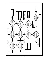
Page 19: ...ut signal mode Check the Input Y Cb Cr At the pin no 5 7 9 of IC AN15865 on Jack board Check the Condition of all Connectors wafers I2C In component Signal flow Power Error Replace IC1 AN15865 To sheet 24 To sheet 25 Yes NO Yes FAIL PASS component PASS S Video FAIL FAIL PASS PASS PASS FAIL NO Check the output YUV at R 418 415 412 respectively Check 9V Across L401and 5V across L404 and L402 ...

Page 20: ... is the input signal mode Check main CVBS at R303 Check Secondary CVBS at R434 for PiP Check 9V Across L401and at pin 3 of IC100 5V across L404 L402 Check 9V Across L401and at pin 3 of IC100 5V across L404 L402 Check the input video signal at pin 48 50 52 54 60 of AN15865 For RF AV1 2 3 IDTV Resp Check the Condition of all Connectors wafers I2C In corresponding Signal flow Yes NO Yes FAIL PASS FAI...

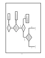
Page 21: ...nd IC203 for HDMI Check the Condition of all Connectors wafers I2C In corresponding Signal flow Power Error Replace IC1 AN15865 To sheet 25 Yes Yes Yes FAIL FAIL FAIL PASS PASS PASS PASS PASS FAIL FAIL Check the interfacing ckt Of corresponding mode On jack board NO Check the input TMDS signal at pins 39 52 for DVI and 58 71 for HDMI of IC601 SiI9021 Check 24 Bit RGB output Across AR 601 606 Check...

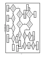
Page 22: ...rect them What is the input signal mode Check the i p RGB HV signal At the pin no 72 76 for X studio and 1 2 78 80 For PC of AN15865 Check the Condition of all Connectors wafers I2C and slots In corres Ponding Signal flow Power Error Replace IC1 AN15865 To sheet 24 Yes NO Yes FAIL PASS FAIL FAIL PASS PASS PASS FAIL NO Check the output YUV at R 418 415 412 respectively Check 9V Across L401and 5V ac...

Page 23: ...of ADC X98014 across RA500 501 Check the 3 3V supply volt across L503 L504 And clock frequency at pin 39 40 of ADC From sheet 23 From sheet 20 To sheet 25 DVI PC X Studio To sheet 25 component Power Error Replace ADC PASS PASS PASS FAIL FAIL ...

Page 24: ...put for PiP at pin 37 41 45 47 for main image at pin 48 46 42 38 of IC902 LVDS IC check 3 3Vdd and 2 5Vdd across respectively LIP2 and LIP1 check the 3 3Vdd across CF12 and 1 8Vdd across CF27 CF33 and 13 5 MHz at pin 191 192 of Froudja Replace Froudja Replace PW181 Power Error Power Error Replace LVDS Replace IEP Crystal or Power Error Replace VSP9437B Crystal or Power Error Crystal or Power Error...

Page 25: ...cross RA18 20 22 if PiP is digital or CVBS at R434 if PiP is RF AV at AN15865 Is PiP mode ON What is the PIP input Push PiP key Change the input for PiP Follow the corresponding Troubleshooting Procedure for same mode To sheet 25 To sheet 21 NO Not Supported PASS FAIL Any other DTV RF AV Supported Yes ...

Page 26: ... supply across L305 and 2 5V at L304 Check the PWM output of NSP across R325 328 Is Mute ON Is the Set ON Correct them Replace NSP Power Error Replace TAS5122 amp Power Error Check the Amplifier output level At L300 303 There may be some error in Audio source Increase the Volume Turn OFF the Mute Push the POWER ON key Check the interfacing ciruit of PC audio Analog Tuner Front AV board Side AV boa...

Page 27: ... NSP across R325 328 Check the Amplifier output level At L300 303 Check 3 3V supply across L305 and 2 5V at L304 Check 18V supply at pin 55and pin 30 of AMP Is the Set ON No power LED indicator off Replace the MSP Power Error Increase the Volume Turn OFF the Mute Replace IC907 Power Error Power Error Replace NSP Push the POWER ON key There may be some error in PC input Replace TAS5122 amp Check th...

Page 28: ... output of NSP across R325 328 Check the Amplifier output level At L300 303 Check 3 3V supply across L305 and 2 5V at L304 Check 18V supply at pin 55and pin 30 of AMP Is the Set ON Correct them Replace the MSP Power Error Increase the Volume Turn OFF the Mute Replace IC907 Power Error Power Error Replace NSP Push the POWER ON key There may be some error in PC input Replace TAS5122 amp Check the in...

Page 29: ... COM0 1SCL SDA M COM0 1SCL SDA S RX TX RX TX P RX TX M RX TX S 656 8BIT Y C H V SYNC Digital 656 8BIT Y C H V SYNC SW 656 8BIT Y C H V SYNC TEXT R G B FB M2 CVBS R G B FB YUV 4 2 2 16BIT CLK H V SYNC V G RGB 8 8 8 DE CLK H V SYNC RGB 8 8 8 DE CLK H V SYNC RGB 8 8 8 IIC PWR0 1 VFD CS DA CLK PANEL S W INV CTL AV ID IR SND MUTE H V SYNC RX TX TMDS DV I TMDS HDMI IIS LR CLK LR CH SCK MCLK IIS DTV IIS ...

Page 30: ...CART AV 2 from half SCART and AV 3 from front A V The SCART Audio AV1 AV2 are fed to MSP4410K through the LA7222 switch for selecting appropriate mode while Front LR AV3 is directly fed to the MSP4410K sound processor IC After these operations the audio and video signals follow the same signal flow and processing as in case of RF Analog input 4 Component mode Initially the video signal is fed to t...

Page 31: ...IAGRAM Wiring Part List NO PART NO 1 6631T11020A 2 6631T11020Z 3 6631T25023N 4 6631T20039C 5 6631T25019N 6 6631T25024Q 7 6631T25023L 8 6631T20037D 9 6631T20032U 10 6631T11022B 11 6631T11023A 12 6631T20034V 13 6631T12007D 14 6631T20028W 15 6631T20034U 16 6631T20033D 17 6631T20028V 18 6631T20028X 21 6852TAZ012J 22 6852TAZ012W ...

Page 32: ... 33 EXPLODED VIEW 010 020 040 160 180 210 120 130 150 151 060 080 090 170 100 110 030 050 140 070 190 200 ...

Page 33: ...A ZA SUB TOTAL BRAND DIGITAL BOARD ASSY 4951TKK276E Plate Assembly SHIELD AV ASSY 37LP1D EA C SKD 68719ST785A PCB Assembly Sub SUB T T ML03JB EA ZA SIDE TOTAL 4951TKK276E Plate Assembly SHIELD AV ASSY 37LP1D EA C SKD 3551TKK586H Cover Assembly 37LP1DA ZA REAR BRACKET AV ASSY EAB31759206 Speaker System 3551TKS063F 4810TKS009A Bracket MOLD ABS 37LP10 SPEAKER DECO RIGHT 4810TKS009B Bracket MOLD ABS 3...

Page 34: ...K6 3TP16VC100M 100uF 20 DATE 2006 02 14 S AL LOC NO PART NO DESCRIPTION SPECIFICATION C9 0CE106VF6DC VGV106M016S0ANB010 10uF 20 C905 0CE107WH6DC MVK8 0TP25VC100M 100uF 20 C908 0CE107WF6DC MVK6 3TP16VC100M 100uF 20 C923 0CE106VF6DC VGV106M016S0ANB010 10uF 20 C925 0CE107WF6DC MVK6 3TP16VC100M 100uF 20 C927 0CE107WF6DC MVK6 3TP16VC100M 100uF 20 C930 0CE477WF6DC MVK10TP16VC470M 470uF 20 1 C97 0CE477WF...

Page 35: ... 0805B104K500CT 100nF 10 50 C603 0CH3104K566 0805B104K500CT 100nF 10 50 C605 0CH3104K566 0805B104K500CT 100nF 10 50 DATE 2006 02 14 S AL LOC NO PART NO DESCRIPTION SPECIFICATION C606 0CH3104K566 0805B104K500CT 100nF 10 50 C61 0CH2473K516 0805B473K500CT 47nF 10 50V C611 0CH6102K406 C2012S2L1H102JT 1nF 5 50V C612 0CH6102K406 C2012S2L1H102JT 1nF 5 50V C613 0CH6102K406 C2012S2L1H102JT 1nF 5 50V C614 0...

Page 36: ...50 CIP11 0CH3104K566 0805B104K500CT 100nF 10 50 CIP12 0CH3104K566 0805B104K500CT 100nF 10 50 DATE 2006 02 14 S AL LOC NO PART NO DESCRIPTION SPECIFICATION CIP13 0CH3104K566 0805B104K500CT 100nF 10 50 CIP14 0CH3104K566 0805B104K500CT 100nF 10 50 CIP15 0CH3104K566 0805B104K500CT 100nF 10 50 CIP16 0CH3104K566 0805B104K500CT 100nF 10 50 CIP2 0CH3104K566 0805B104K500CT 100nF 10 50 CIP3 0CH3104K566 0805...

Page 37: ...73K516 0805B473K500CT 47nF 10 50V C63 0CH2473K516 0805B473K500CT 47nF 10 50V C64 0CH2473K516 0805B473K500CT 47nF 10 50V C65 0CH2473K516 0805B473K500CT 47nF 10 50V C69 0CH2473K516 0805B473K500CT 47nF 10 50V DATE 2006 02 14 S AL LOC NO PART NO DESCRIPTION SPECIFICATION C702 0CH6100K116 C2012C0G1H100DT 10pF 0 5PF C74 0CH2473K516 0805B473K500CT 47nF 10 50V C75 0CH2473K516 0805B473K500CT 47nF 10 50V C8...

Page 38: ...R602 6210TCE002B HB 4M3216 121JT 120OHM 3 2X AR603 6210TCE002B HB 4M3216 121JT 120OHM 3 2X DATE 2006 02 14 S AL LOC NO PART NO DESCRIPTION SPECIFICATION AR604 6210TCE002B HB 4M3216 121JT 120OHM 3 2X AR605 6210TCE002B HB 4M3216 121JT 120OHM 3 2X AR606 6210TCE002B HB 4M3216 121JT 120OHM 3 2X AR607 6210TCE002B HB 4M3216 121JT 120OHM 3 2X AR608 6210TCE002B HB 4M3216 121JT 120OHM 3 2X L13 6210TCE001G H...

Page 39: ... MCR10EZHJ332 3 3KOHM 5 1 8 DATE 2006 02 14 S AL LOC NO PART NO DESCRIPTION SPECIFICATION R129 0RH3301D622 MCR10EZHJ332 3 3KOHM 5 1 8 R137 0RH1500D622 MCR10EZHJ151 150OHM 5 1 8W R138 0RH0682D622 MCR10EZHJ680 68OHM 5 1 8W R139 0RH1500D622 MCR10EZHJ151 150OHM 5 1 8W R140 0RH0682D622 MCR10EZHJ680 68OHM 5 1 8W R164 0RH3301D622 MCR10EZHJ332 3 3KOHM 5 1 8 R165 0RH4702D622 MCR10EZHJ473 47KOHM 5 1 8W R166...

Page 40: ...RH3301D622 MCR10EZHJ332 3 3KOHM 5 1 8 R942 0RH3301D622 MCR10EZHJ332 3 3KOHM 5 1 8 DATE 2006 02 14 S AL LOC NO PART NO DESCRIPTION SPECIFICATION R943 0RH3301D622 MCR10EZHJ332 3 3KOHM 5 1 8 R944 0RH3301D622 MCR10EZHJ332 3 3KOHM 5 1 8 R945 0RH3301D622 MCR10EZHJ332 3 3KOHM 5 1 8 R946 0RH3301D622 MCR10EZHJ332 3 3KOHM 5 1 8 R95 0RH3301D622 MCR10EZHJ332 3 3KOHM 5 1 8 R952 0RH3301D622 MCR10EZHJ332 3 3KOHM...

Page 41: ...102 1KOHM 5 1 8W R17 0RH1000D622 MCR10EZHJ101 100OHM 5 1 8W R170 0RH1001D622 MCR10EZHJ102 1KOHM 5 1 8W DATE 2006 02 14 S AL LOC NO PART NO DESCRIPTION SPECIFICATION R171 0RH1000D622 MCR10EZHJ101 100OHM 5 1 8W R173 0RH1000D622 MCR10EZHJ101 100OHM 5 1 8W R175 0RH1000D622 MCR10EZHJ101 100OHM 5 1 8W R177 0RH1000D622 MCR10EZHJ101 100OHM 5 1 8W R178 0RH1000D622 MCR10EZHJ101 100OHM 5 1 8W R181 0RH0752D62...

Page 42: ... 1 8W R71 0RH0000D622 MCR10EZHJ000 0OHM 5 1 8W 2 R72 0RH0752D622 MCR10EZHJ750 75OHM 5 1 8W DATE 2006 02 14 S AL LOC NO PART NO DESCRIPTION SPECIFICATION R752 0RH0222D622 MCR10EZHJ220 22OHM 5 1 8W R753 0RH0222D622 MCR10EZHJ220 22OHM 5 1 8W R755 0RH0222D622 MCR10EZHJ220 22OHM 5 1 8W R756 0RH0222D622 MCR10EZHJ220 22OHM 5 1 8W R757 0RH0222D622 MCR10EZHJ220 22OHM 5 1 8W R758 0RH0222D622 MCR10EZHJ220 22...

Page 43: ...609 RD 96T1J100R 100OHM 5 1 6W C1201 0CH3104K566 0805B104K500CT 100nF 10 50 C1202 0CH3104K566 0805B104K500CT 100nF 10 50 C1203 0CH3104K566 0805B104K500CT 100nF 10 50 C1204 0CH3104K566 0805B104K500CT 100nF 10 50 C1205 0CH3104K566 0805B104K500CT 100nF 10 50 C1206 0CH3104K566 0805B104K500CT 100nF 10 50 C1207 0CH3104K566 0805B104K500CT 100nF 10 50 C1208 0CH3104K566 0805B104K500CT 100nF 10 50 C1216 0CH...

Page 44: ...P1289 1C1P 15VDC 0 02A VE SW1208 6600R00001B JTP1289 1C1P 15VDC 0 02A VE C2103 0CH6102K406 C2012S2L1H102JT 1nF 5 50V DATE 2006 02 14 S AL LOC NO PART NO DESCRIPTION SPECIFICATION C2104 0CH6102K406 C2012S2L1H102JT 1nF 5 50V CF1 0CH3104K566 0805B104K500CT 100nF 10 50 CF4 0CH6102K406 C2012S2L1H102JT 1nF 5 50V CF5 0CH6102K406 C2012S2L1H102JT 1nF 5 50V L2108 6210TCE001A HB 1S2012 080JT 8OHM 2X1 25 L210...

Page 45: ...500CT 100nF 10 50 C62 0CH3104K566 0805B104K500CT 100nF 10 50 C63 0CH3104K566 0805B104K500CT 100nF 10 50 DATE 2006 02 14 S AL LOC NO PART NO DESCRIPTION SPECIFICATION C64 0CH3104K566 0805B104K500CT 100nF 10 50 C65 0CH3104K566 0805B104K500CT 100nF 10 50 C66 0CH3104K566 0805B104K500CT 100nF 10 50 C67 0CH3104K566 0805B104K500CT 100nF 10 50 C7 0CH3104K566 0805B104K500CT 100nF 10 50 C78 0CH6470K416 C201...

Page 46: ...A86TRJ22R0 22OHM 5 1 16W AR305 0RJ0222C687 RCA86TRJ22R0 22OHM 5 1 16W DATE 2006 02 14 S AL LOC NO PART NO DESCRIPTION SPECIFICATION AR306 0RJ0222C687 RCA86TRJ22R0 22OHM 5 1 16W AR307 0RJ0222C687 RCA86TRJ22R0 22OHM 5 1 16W AR308 0RJ0222C687 RCA86TRJ22R0 22OHM 5 1 16W AR309 0RJ0222C687 RCA86TRJ22R0 22OHM 5 1 16W AR310 0RJ0222C687 RCA86TRJ22R0 22OHM 5 1 16W AR311 0RJ0222C687 RCA86TRJ22R0 22OHM 5 1 16...

Page 47: ...32D622 MCR10EZHJ330 33OHM 5 1 8W R103 0RH0332D622 MCR10EZHJ330 33OHM 5 1 8W DATE 2006 02 14 S AL LOC NO PART NO DESCRIPTION SPECIFICATION R104 0RH0332D622 MCR10EZHJ330 33OHM 5 1 8W R105 0RH0332D622 MCR10EZHJ330 33OHM 5 1 8W R106 0RH0332D622 MCR10EZHJ330 33OHM 5 1 8W R107 0RH0332D622 MCR10EZHJ330 33OHM 5 1 8W R108 0RH0332D622 MCR10EZHJ330 33OHM 5 1 8W R11 0RH4701D622 MCR10EZHJ472 4 7KOHM 5 1 8 R114...

Page 48: ...HM 3 2X DATE 2006 02 14 S AL LOC NO PART NO DESCRIPTION SPECIFICATION B8 6210TCE001G HH 1M3216 501JT 500OHM 3 2X B9 6210TCE001G HH 1M3216 501JT 500OHM 3 2X C204 0CH3104K566 0805B104K500CT 100nF 10 50 C208 0CH6101K416 C2012C0G1H101JT 100pF 5 50 C209 0CH6101K416 C2012C0G1H101JT 100pF 5 50 C210 0CH6331K416 C2012C0G1H331JT 330pF 5 50 C211 0CH6331K416 C2012C0G1H331JT 330pF 5 50 C220 0CH6331K416 C2012C0...

Page 49: ... HH 1M3216 501JT 500OHM 3 2X L402 6210TCE001G HH 1M3216 501JT 500OHM 3 2X L403 6210TCE001G HH 1M3216 501JT 500OHM 3 2X DATE 2006 02 14 S AL LOC NO PART NO DESCRIPTION SPECIFICATION L404 6210TCE001G HH 1M3216 501JT 500OHM 3 2X L500 6210TCE001G HH 1M3216 501JT 500OHM 3 2X L501 6210TCE001G HH 1M3216 501JT 500OHM 3 2X L502 6210TCE001G HH 1M3216 501JT 500OHM 3 2X L503 6210TCE001G HH 1M3216 501JT 500OHM...

Page 50: ...5 1 8W R401 0RH0000D622 MCR10EZHJ000 0OHM 5 1 8W 2 R404 0RH0000D622 MCR10EZHJ000 0OHM 5 1 8W 2 DATE 2006 02 14 S AL LOC NO PART NO DESCRIPTION SPECIFICATION R406 0RH0000D622 MCR10EZHJ000 0OHM 5 1 8W 2 R408 0RH0000D622 MCR10EZHJ000 0OHM 5 1 8W 2 R409 0RH2201D622 MCR10EZHJ222 2 2KOHM 5 1 8 R413 0RH2200D622 MCR10EZHJ221 220OHM 5 1 8W R416 0RH2200D622 MCR10EZHJ221 220OHM 5 1 8W R426 0RH3900D622 MCR10E...

Page 51: ...00M 100uF 20 C101 0CE107WF6DC MVK6 3TP16VC100M 100uF 20 C102 0CE107WF6DC MVK6 3TP16VC100M 100uF 20 DATE 2006 02 14 S AL LOC NO PART NO DESCRIPTION SPECIFICATION C103 0CE107WF6DC MVK6 3TP16VC100M 100uF 20 C107 0CE107WF6DC MVK6 3TP16VC100M 100uF 20 C108 0CE476WF6DC MVK6 3TP16VC47M 47uF 20 16 C109 0CE107WF6DC MVK6 3TP16VC100M 100uF 20 C110 0CE107WF6DC MVK6 3TP16VC100M 100uF 20 C2 0CH3224K946 C2012Y5V...

Page 52: ...J TE13 2KBIT 256X8 IC203 0ICS240213A CAT24WC02J TE13 2KBIT 256X8 IC204 0ISTLFA058A 74F14SCX 4 5TO5 5V 25mA SCH DATE 2006 02 14 S AL LOC NO PART NO DESCRIPTION SPECIFICATION IC206 0IMMRCS013A CAT24C21 1KBIT 128X8BIT 2 5 IC207 0ISTL00026A MC14066BDR2G 3TO18V 0 001mA IC502 0IMCRSH001A PQ05DZ1U 6TO16V 5V 8W D2PAK IC602 0IMCRMN028B MSP4410K 3 1TO3 5V_4 75TO5 IC603 0IMCRTI001A SN74HCT157DR 4 5TO5 5V 0 0...

Page 53: ...0EZHJ222 2 2KOHM 5 1 8 R653 0RH2201D622 MCR10EZHJ222 2 2KOHM 5 1 8 R654 0RH4700D622 MCR10EZHJ471 470OHM 5 1 8W R657 0RH2200D622 MCR10EZHJ221 220OHM 5 1 8W DATE 2006 02 14 S AL LOC NO PART NO DESCRIPTION SPECIFICATION R658 0RH1001D622 MCR10EZHJ102 1KOHM 5 1 8W R659 0RH1001D622 MCR10EZHJ102 1KOHM 5 1 8W R660 0RH0000D622 MCR10EZHJ000 0OHM 5 1 8W 2 R676 0RH2201D622 MCR10EZHJ222 2 2KOHM 5 1 8 R680 0RH2...

Page 54: ...Y NPN 5V 60V 50 Q104 0TFON80009A NTS2101PT1G P CHANNEL MOSFE Q105 0TFON80004C NTR4501NT1G N CHANNEL MOSFE DATE 2006 02 14 S AL LOC NO PART NO DESCRIPTION SPECIFICATION R102 0RJ0222D677 MCR03EZPJ220 22OHM 5 1 10W R104 0RJ0222D677 MCR03EZPJ220 22OHM 5 1 10W R107 0RJ1000D677 MCR03EZPJ101 100OHM 5 1 10 R108 0RJ1000D677 MCR03EZPJ101 100OHM 5 1 10 R109 0RJ1002D677 MCR03EZPJ103 10KOHM 5 1 10 R111 0RJ4701...

Page 55: ...30A00 30P 1 25MM 1R IC101 0IPRPAL005A AT76C120 UI OJZ208 1 8VTO3 IC102 0IZZTSA116A ATMEL 48P 37LP1DA ZA X STUD DATE 2006 02 14 S AL LOC NO PART NO DESCRIPTION SPECIFICATION IC103 0TR830009BA BSS83 N CHANNEL MOSFET 10V IC105 0IPRPPH041A UDA1334BTS 1 8VTO3 6V 44 1K IC106 0TR830009BA BSS83 N CHANNEL MOSFET 10V IC107 0TRON80020A NUS2401SNT1G PNP NPN 7V 7V IC108 0IPMGS1012A SC1592ISTRT 3TO16V 1 8V S IC...

Page 56: ...0058AA NSCW215T WHITE 4 0V 30mA 36 C3100 0CE106SF6DC VMV106M016S0ANB010 10uF 20 C3101 0CE106SF6DC VMV106M016S0ANB010 10uF 20 C3102 0CE106SF6DC VMV106M016S0ANB010 10uF 20 C3103 0CE106SF6DC VMV106M016S0ANB010 10uF 20 C3104 0CE106SF6DC VMV106M016S0ANB010 10uF 20 C3105 0CE106SF6DC VMV106M016S0ANB010 10uF 20 C3106 0CE106SF6DC VMV106M016S0ANB010 10uF 20 C3107 0CE106SF6DC VMV106M016S0ANB010 10uF 20 C3108...

Page 57: ......

Page 58: ......

Page 59: ......

Page 60: ......

Page 61: ...Fer 2006 Printed in Korea P NO ...

Reviews: