


MIPI DSI to OpenLDI/FPD-Link/LVDS Interface Bridge Soft IP
User Guide
© 2016 Lattice Semiconductor Corp. All Lattice trademarks, registered trademarks, patents, and disclaimers are as listed at
. All other brand or product names are
trademarks or registered trademarks of their respective holders. The specifications and information herein are subject to change without notice.
FPGA-IPUG-02003-1.2
13
2.8.
Reset and Clocking
Asynchronous active low reset input (reset_n_i) is used as a system reset. Local reset signals are derived from the
system reset to create asynchronous reset assertion and synchronous reset deassertion for logic in different clock
domains (non-continuous byte clock not included). Logic in continuous byte clock and pixel clock domains are also reset
when ready_o from lvds_wrapper is low. Logic in LVDS wrapper is reset when PLL lock is low. The system reset input
must be asserted for at least 60 ns.
Internal PLL could take ~15 ms to be locked after PLL reference clock is made available. Data loss is expected when
incoming MIPI DSI transaction begins during this period when PLL lock is not yet obtained. To avoid malfunction, the
MIPI DSI to OpenLDI/FPD-Link/LVDS Interface Bridge IP discards any received MIPI DSI packets until it detects “VSYNC
start” short packet.
When MIPI D-PHY clock is continuous, it is expected to be in high speed mode at power on of the device. The HS
termination enable of clock lane is tied to VCC. Continuous byte clock is generated by hard D-PHY IP and used as PLL
reference clock. Internal PLL generates eclk used to serialize data. A clock divider is used to generate pixel clock inside
the lvds wrapper.
When MIPI D-PHY clock is non-continuous, an external clock source (clk_ref_i) is needed for PLL reference clock.
Internal PLL generates continuous byte clock and eclk. Internal oscillator clock is used to detect LP to HS transition of
clock lane and for reset synchronization sequence of DDR components inside lvds wrapper. Internal oscillator
generates ~48 MHz clock.
Maximum fabric clock of CrossLink device is 150 MHz while maximum continuous byte clock is 112.5 MHz due to heavy
logic inside capture controller and byte2pixel core modules. Rx gear 16 and Tx gear 14 features are added to achieve
higher data rates by doubling the parallel data bus width and dividing byte clock and pixel clock by 2, respectively.
For single Rx to single Tx and dual Rx to dual Tx configurations, the Rx line rate is limited by maximum Tx line rate that
is 1.2 Gb/s.
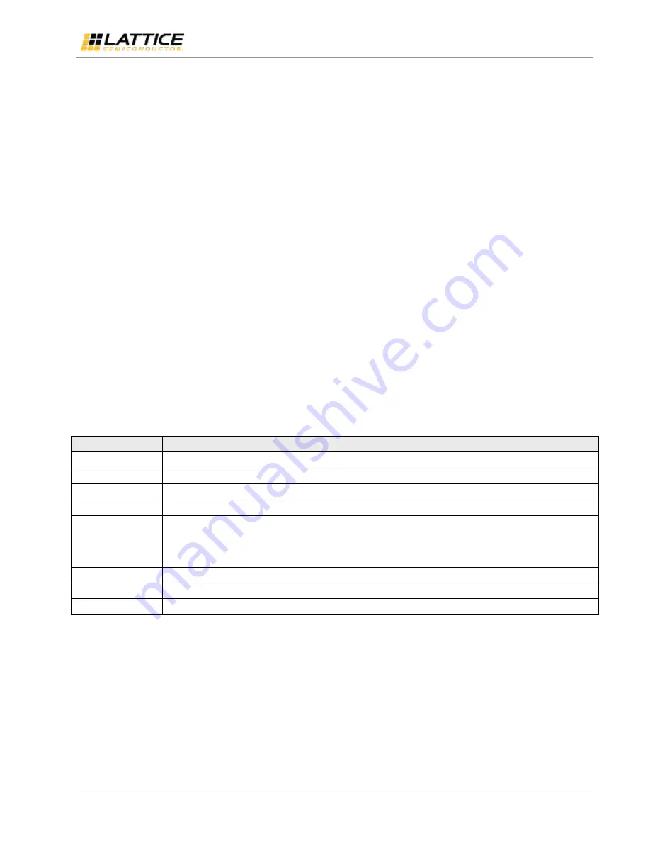
Frequency calculations are given in
. DCK refers to MIPI D-PHY clock frequency.
Table 2.3. Clock Frequency Calculations
Clock
Formula
Rx line rate
DCK * 2
Tx line rate
LVDS Output clock * 7
D-PHY clock
DCK
Byte clock
DCK / (RX_GEAR/2)
Pixel clock
Byte clock * Rx lanes * RX_GEAR / (Pixel width * Pixels per pixel clock cycle) , where pixels per pixel clock
cycle is:
TX_GEAR/7 – for single Rx to single Tx or dual Rx to dual Tx
TX_GEAR/3.5 – for single Rx to dual Tx
eclk
Pixel clock * (TX_GEAR/2)
LVDS output clock
Pixel clock * (TX_GEAR/7)
Reference clock
Byte clock