NXR-710
16
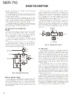
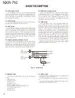
4-6. Power supply voltage monitoring circuit
The X53-449 circuit consists of IC307, IC308, D303 and
Q301.
IC308 is a voltage detect IC and is used to generate the
“/RST” signal for the MCU (IC20).
This “/RST” signal is connected to the hardware reset
pin of MCU (IC20).
IC307 is a voltage detect IC and is used to generate the
“/BINT” signal for the MCU (IC20).
This “/BINT” signal is connected to the hardware inter-
rupt pin of MCU (IC20). The software of the MCU (IC20)
runs to the sleep-mode to use the “/BINT” signal.
D303 and Q301 are used to generate the “OVRB” signal
for the MCU (IC20). The software of the MCU (IC20) runs to
the sleep-mode to use the “OVRB” signal.
SW
SW
CN301
DC-DC
IC301
RESET
IC308
AVR
IC302
AVR
IC303
60DC
33M
AVR
IC305
16M
AVR
IC304
15M
/BINT
IC307
/BINT
/OVRB
Q301
OR
Q401
/OVRB
AVR
IC306
33A
50M
/RST
Q303
33BU
Q402
AMP_B
AMP_SW
B
SB
Fig. 15 Power supply circuit
4-7. 18.432MHz clock circuit
The 18.432MHz clock is provided to the MCU (IC20),
DSP(IC6), and DAC (IC14) of the Squelch circuit.
4-8. Audio circuit
■
Audio amplifi er circuit
The audio amplifi er circuit is located in the control sec-
tion of the Control unit (X53-449). The 4W output audio
power is available from the pin 15 TEST/SPKR connector
“SPO”, “SPG” on the rear panel to the external speaker in
the case of a power supply voltage of 13.6V and a 4
Ω
load.
■
Microphone circuit
The signal from the microphone is passed through the
AGC circuit located in the Display unit (X54-358 A/2) so that
it may not saturate. This circuit consists of IC501, D501,
D502 Q501, and Q502. The AGC controls the amplifi er gains
using the detected audio signal depending on the positive
and negative peaks of the signal amplitude. The audio sig-
nal goes to the control section of the Control unit (X53-449)
from the Display unit (X54-358 A/2).
■
Modulation circuit (Analog/Digital signal processing)
In the case of the Analog Signal Processing mode, the
transmitting audio signal is amplifi ed by IC405 (C/4), input to
the MICADCO terminal of the MCU (IC20), and audio pro-
cessed by DSP (IC6). The processed audio signal from the
MODDAC terminal of IC20 is passed through an anti-aliasing
fi lter at IC404 (A/2), and is then amplifi ed to a suffi cient level
by IC404 (B/2), and amplifi ed by the summing (TD) amplifi er.
The Digital Signal Processing mode is the same as the Ana-
log Signal Processing mode.
4-9. Other circuit
■
Real-time clock
The clock function is based on a real-time clock IC (IC17).
When the power supply is off, it is backed up by an internal
secondary lithium battery.
CIRCUIT DESCRIPTION

