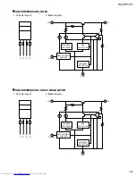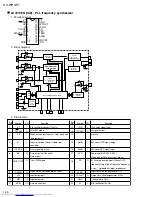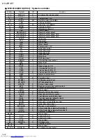
RS-WP1WT
1-27
30
16
~
1
15
~
4
3
2
1
30
29
28
27
26
25
24
23
22
21
20
19
18
17
16
15
14
13
12
11
10
9
8
8
7
5
CONTROL
CIRCUIT
CONTROL
CIRCUIT
LOGIC
CIRCUIT
CCB
INTERFACE
LVref
RVref
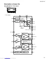
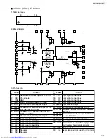
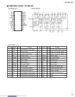
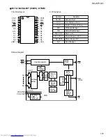
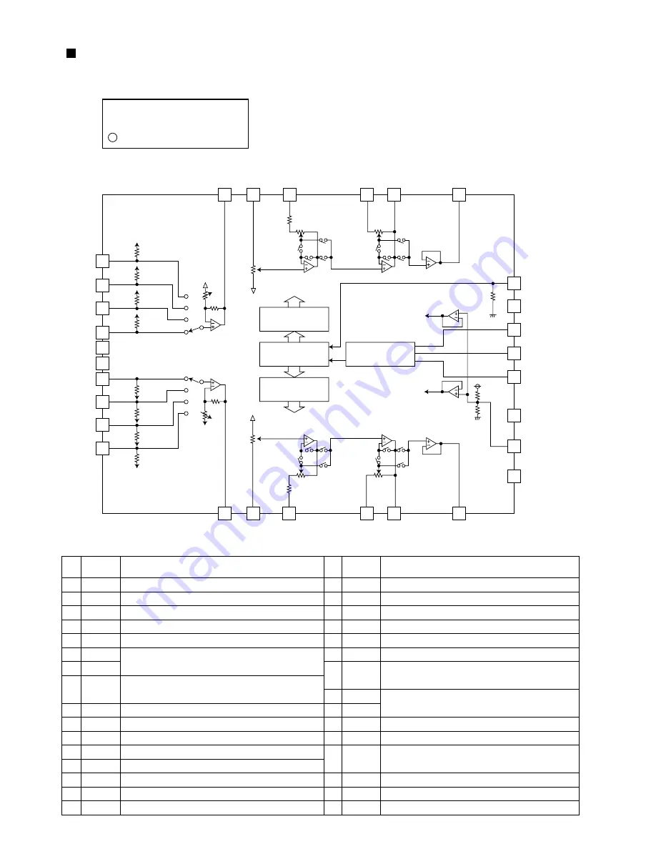
LC75342 (IC501) : E. volume
2. Block diagram
3. Pin function
1. Terminal layout
1
2
3
4
5
6
7
8
9
10
11
12
13
14
15
16
Serial data and clock input for IC control
Chip enable
GND
Electric volume connection for test
Volume control and equalizer input
Connection for resistor and capacitor that
from the bass band filter
Connection for capacitor that from the
treble band filter
Volume control and equalizer input
Input selector output
Input signal connections
Input signal connections
Input signal connections
Input signal connections
Not used
Not used
DI
CE
VSS
TEST
LOUT
LBASS2
LBASS1
LTRE
LIN
LSEL0
L4
L3
L2
L1
NC
NC
17
18
19
20
21
22
23
24
25
26
27
28
29
30
R1
R2
R3
R4
RSEL0
RIN
RTRE
RBASS1
RBASS2
ROUT
NC
Vref
VDD
CL
Pin
No.
Pin
No.
Symbol
Symbol
Function
Input signal connections
Input signal connections
Input signal connections
Input signal connections
Input selector output
Volume control and equalizer input
Connection for capacitor that from the treble
band filter
Connection for resistor and capacitor that from
the bass band filter
Volume control and equalizer input
Not used
Connection to the 0.5X VDD voltage generator
circuit used as the analog signal ground
Power supply
Serial data and clock input for IC control
Function
Summary of Contents for RS-WP1WT
Page 37: ...RS WP1WT 3 2 M E M O ...
Page 57: ...RS WP1WT 2 4 ...
Page 66: ...RS WP1WT 2 13 Tuner Board Block No 04 ...
Page 68: ...RS WP1WT 2 15 ...

