RS-WP1WT
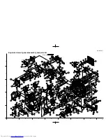
1-23
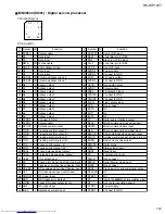
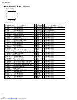
10
21
20
2
3
4
1
18
19
17
22
23
11
15
14
12
13
16
7
5
6
8
9
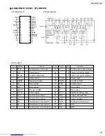
Standby SW
Switching
regulator block
CH 1
CH 2
ON MUTE
muting circuit
Pop noise
prevention circuit
Nonlinear amplifier/output stage
Power supply/ground shorting
protection circuit
Overvoltage/thermal protection
circuit
Input amplifier
BEEP
amplifier
Input amplifier
A
B
D
C
Nonlinear/output stage
Amplifier output stage
SW
drive
A B C D
H.L.S.
STBY
D.C
PRE GND
IN 1
IN 2
ON TIME
BEEP
Vcc
Vcc(SW)
SW B
SW E
SW OUT1
SW OUT2
SW GND
+OUT 1
+OUT 2
N.C.
-OUT 1
-OUT 2
PWR GND 1
PWR GND 2
H.L.S. :
Higher
Level signal
selector
Ripple
filter
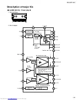
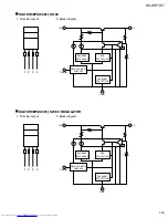
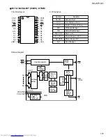
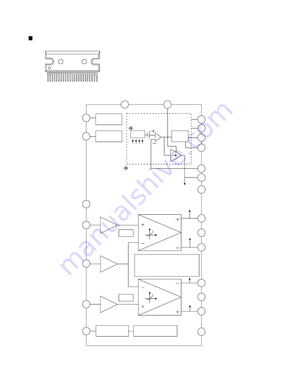
LA4905 (IC101) : Power amp IC
1. Terminal layout
2. Block diagram
1
23
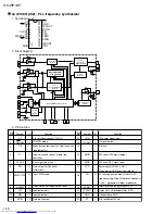
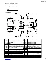
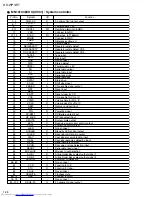
Description of major ICs
Summary of Contents for RS-WP1WT
Page 37: ...RS WP1WT 3 2 M E M O ...
Page 57: ...RS WP1WT 2 4 ...
Page 66: ...RS WP1WT 2 13 Tuner Board Block No 04 ...
Page 68: ...RS WP1WT 2 15 ...

