background image

1-5

Disassembly method

Commence disassembly of this set by re

moving the main units a

nd then proceed to the components a

nd

assemblies inside the units.


Replacement of the fuses and the power IC

 Top cover
 CD changer unit
 Front panel assembly
 Chassis unit

 CD changer unit

 Removing the main PCB
 Removing the CD changer mechanism assembly
 Removing the CD pickup
 Replacing the loading motor and belt of the CD changer tray
 Replacing the CD tray rotor belt of CD changer, and removing the motor

 Front panel assembly

 Removing the cassette deck mechanism
 Removing the earphone jack PCB
 Removing the control/FL  PCB
 Removing the switch PCB and ACTIVE BASS EX. switch PCB
 Removing the cassette deck main motor, and replacing the main belts
 Removing the leaf switches of the cassette deck mechanism
 Removing the cassette deck heads

 Chassis unit

 Removing the 3-pin regulator
 Removing the power amp and supply PCB and the Power Trans PCB
 Removing the sub power PCB

Summary of Contents for MX-K10/30

Page 1: ...laser pickup Replacement of laser pickup Description of major ICs 1 20 1 21 1 21 1 22 Safety precautions Important for laser products Preventing static electricity Disassembly method Adjustment method 1 2 1 3 1 4 1 5 1 18 Contents COPYRIGHT 2001VICTOR COMPANY OF JAPAN LTD Area Suffix U ASIA UW LATIN AMERICA MX K10 30 TENTATIVE ...

Page 2: ... related characteristics These characteristics are often not evident from visual inspection nor can the protection afforded by them necessarily be obtained by using replacement components rated for higher voltage wattage etc Replacement parts which have these special safety characteristics are identified in the Parts List of Service Manual Electrical components having such features are identified ...

Page 3: ...and is equipped with safety switches which prevent emission of radiation when the drawer is open and the safety interlocks have failed or are defeated It is dangerous to defeat the safety switches 5 CAUTION If safety switches malfunction the laser is able to function 6 CAUTION Use of controls adjustments or perfor mance of procedures other than those specified herein may result in hazardous radiat...

Page 4: ...e text 2 Do not use a tester to check the condition of the laser diode in the optical pickup The tester s internal power source can easily destroy the laser diode 4 Handling the CD changer unit optical pickup 1 Do not subject the CD changer unit optical pickup to strong shocks as it is a sensitive complex unit 2 Cut off the shorted part of the flexible cable using nippers etc after replacing the o...

Page 5: ... loading motor and belt of the CD changer tray Replacing the CD tray rotor belt of CD changer and removing the motor Front panel assembly Removing the cassette deck mechanism Removing the earphone jack PCB Removing the control FL PCB Removing the switch PCB and ACTIVE BASS EX switch PCB Removing the cassette deck main motor and replacing the main belts Removing the leaf switches of the cassette de...

Page 6: ...e left side BOARD and remove tuner PCB Fig 4 BB 1 Replace the fuses inside Caution Be sure to use fuses with the specified ratings Replacing the power IC See Fig 2 to 3 Prior to performing the following procedure remove the top cover 1 Remove the two screws A from the heat sinkbetween the power IC 2 Remove the solder fixing the power IC For MX K10 Fig 2 w A For MX K30 Fig 3 W A ...

Page 7: ... cover outward Removing the top cover and two sides BOARD See Fig 5 and 6 1 Remove the six screws C that retain the top cover from the rear of the body 2 Remove the eight screws C and D that retain the top from the two sides of the body 3 Remove the top cover from the body by lifting it toward the rear ...

Page 8: ... mage a From the front pa nel side of this set push in the sec tion s marked with arrows a nd pull out the CD tray toward the front b Remove the CDtray pa nel by pushing both of its ex tremities upward in the direction of the arrows c Push the CD tray deep into the set 1 Disconnect the card wires from the CD PCB CN703 and CN203 2 From the rear of the set remove the two screws E and two serews G on...

Page 9: ...ire from the connectors CN702 CN701 CN101 CN850 on the power a mp and supply PCB 2 Remove the two screws H retaining the front pa nel assembly onto the bottom of the body 3 Remove the screw I retaining the ca ssette de ck mechanism a nd then re move thenGND lug b that comes from the power a mp and supply PCB 4 Disengage the claws c on both side s at the bottom of the front pa nel assembly a nd the...

Page 10: ...4 on the CDPCB which is located on the ba ck side of the CDchanger unit 2 The two screws J that retain the CD PCB should be removed 3 Remove the CD PCB by pulling it toward the side where the CN601 is located 4 Using solder short the CD pickup to connect to short round Caution Afterre conne ctingthe wires be sure to remove the shorting solder from the GND connection 5 Disconnect the card wire from...

Page 11: ...rews d from the front chuch base of the CD changer mechanism unit 2 Turn the CD changer mechanism cover base and re move the screws e connecting the unit to the CD changer mechanism assembly 3 Removing the four screws k retaining the CD mecha nism holder assembly Caution When replacing the CDchanger mechanism assembly be sure not to mistake the posi tions of the silver color and copper color sprin...

Page 12: ...ews L retaining the CD changer tray loading motor 2 Remove the two screws M retaining the gear plate and take it out after remove the rotor belt from the pulley Replacing the CD turn table and remov ing the motor See Fig 20 and 21 Prior to performing the following procedures re move the top cover Also remove the CD changer unit 1 Remove the one screws N retaining the CD Turn table 2 Remove the two...

Page 13: ... to performing the following procedure remove the top cover and both sides board Also remove the CD changer unit Also remove the front panel assembly 1 Remove the screw with the washer P that retains the earphone jack PCB Removing the control FL PCB See Fig 24 Prior to performing the following procedure remove the top cover and both sides board Also remove the CD changer unit Also remove the CD ch...

Page 14: ...remove the front panel assembly 1 Pull out the volume control knob and MIC Volume Knob from the front of the front panel assembly 2 Remove the four screws Q retaining the front panel assembly 3 Remove the control FL PCB 4 Remove the eleven screws R retaining the switch key 1 PCB 5 Remove the three screws S retaining the sound mode key 2 switch PCB 6 Remove two screws T retaining the CD function ke...

Page 15: ...he backside of the cassette deck remove the main motor and two main belts Caution The lengths of the cassette A playback only and cassette B record play main belts are different When attaching the main belts use the longer belt for cassette A Removing the leaf switches of the cas sette deck mechanism See Fig 22 and 30 Prior to performing the following procedures remove the top cover and both sides...

Page 16: ...terminal and disconnect the wire 4 Remove the screw U that retains the head 5 Remove the screw V that retains the head 6 Hold the head and slide it in the direction of the arrow to remove it Removing the 3 pin regulator See Q904 Q907 32 and 33 Prior to performing the following procedures remove the top cover and both sides board 1 Remove the two screws A that connect the heat sink cover to the rea...

Page 17: ...0 screws AA formthe CA MXK10 chassis MX K30backpanel between the heat sink 4 Remove the three screws X that retain the speaker terminals and AUX terminal 5 Remove the screw YY and Y that retains the rear panel andAC switch screw then remove the rear panel 6 Disconnect the parallel wires from the connectors FW951 on the power trans PCB 7 Remove the screw Z that retain the power amp and supply PCB a...

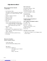
Page 18: ...2121A Fast Forward and Rewind TW2231A 9 Test disc CTS 1000 12cm GRG 1211 8cm 10 Jitter meter Measurement conditions Select correct AC LineVolt Power supply voltage AC110 127 220 230 240V 50 60Hz US UX Measurement output terminal Speaker out TP101 Measuring for TUNER DECK CD Dummy load 6ohm Radio input signal AM modulation frequency 400Hz Modulation factor 30 FM modulation frequency 400Hz Frequency...

Page 19: ...tion frequency to 80KHz 3KHz by core of Oscillation coil of L301 80kHz 3kHz Use the High Impedance Probe or Frequency counter input Items Measurement conditions Measurement method Standard values Adjusting positions AM Tracking Alignments Input signal 530kHz 529kHz 600kHz 603kHz Adjustment point Antenna coil L2 1 Set the Signal Generator signal to 530KHz 529KHz the feed to Loop Antenna 2 Receiving...

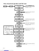
Page 20: ...ffset Laser ON Detection of disc Automatic tuning of Focus offset Automatic measurement of Focus S curve amplitude Power ON Play Key Disc is rotated Focus servo ON Tracking servo ON Automatic measurement of Tracking error amplitude Automatic tuning of Tracking error balance Automatic tuning of Focus error balance Automatic tuning of Focus error gain Automatic tuning of Tracking error gain TOC read...

Page 21: ...3 Semi fixed resistor on the APC PC board The semi fixed resistor on the APC printed circuit board which is attached to the pickup is used to adjust the laser power Since this adjustment should be performed to match the characteristics of the whole optical block do not touch the semi fixed resistor If the laser power is lower than the specified value the laser diode is almost worn out and the lase...

Page 22: ...1 22 Description of major ICs AN22000A IC611 CD DA Head Amp 1 Terminal layout 2 Pin function 3 Block diagram 1 3 2 16 17 ...

Page 23: ...1 23 BA5936S IC621 6 channel BTL driver 1 Block diagram 2 Pin function ...

Page 24: ...02 IC852 Dual operational amplifier 1 Terminal layout block diagram BA3837 IC103 MIC Mixer 1 Terminal layout block diagram 2 Pin function BU9253AS IC851 Low pass filter echo mixer 1 Terminal layout block diagram 2 Pin function ...

Page 25: ...1 25 LA1823DIP IC1 1chip AM FM MPX tuner system 1 Block diagram 2 Pin function ...

Page 26: ...1 26 LC72136N IC2 PLL Frequency synthesizer 1 Terminal layout 2 Block diagram 3 Pin function ...

Page 27: ...1 27 TA8189N IC401 REC PB amp 1 Terminal layout 2 Block diagram 3 Pin function ...

Page 28: ...1 28 TC74HC4094AP IC402 8 bit shift and store resister 1 Terminal layout 2 Block diagram ...

Page 29: ...1 29 TDA7440D IC101 Audio processor 1 Terminal layout 2 Block diagram ...

Page 30: ...1 30 MN662748RPM IC601 Digital servo digital signal processor 1 Terminal layout 2 Pin function ...
Page 31: ...200207 No 21137 VICTOR COMPANY OF JAPAN LIMITED AUDIO COMMUNICATION BUSINESS DIVISION PERSONAL MOBILE NETWORK B U 10 1 1 Chome Ohwatari machi maebashi city 371 8543 Japan MX K10 30 ...

Reviews: