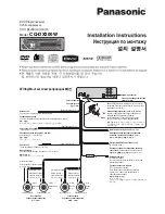
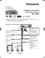
1-22
KS-FX725R
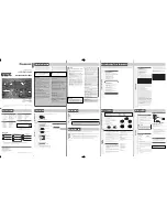
Description of major ICs
UPD178018AGC584(IC701) : System controller micon
24 – 1
41 – 64
25
40
80
65
1.Terminal Layout
2.Description
–
–
1
KEY0
I
Key input 0
2
KEY1
I
Key input 1
3
KEY2
I
Key input 2
4
LEVEL
I
Level meter input
5
SM
I
Signal meter input
6
SQ
I
Signal quality input
7
LCDCE
O
Chip enable output to LCD driver
8
LCDDA
O
Data output to LCD driver
9
LCDSCK
O
Clock output to LCD driver
10
BUSI/O
O
J-BUS I/O switch output
11
UNLOCK
O
PLL unlock output L:unlock H:lock
12
BUSSI
I
J-BUS data input
13
BUSSO
O
J-BUS data output
14
BUSSCK
O
J-BUS clock output
15 - 20
NC
-
Non connect
21
GNDPORT
-
GND for port
22
VDDPORT
-
VDD for port
23
NC
-
Non connect
24
AFCK
O
AF check output L:AF check
25
MONO
O
Monaural ON/OFF output H:Monaural ON
26
FM/AM
O
Output for FM power supply H:FM Mode
27
SEEK/STOP
O
Auto seek/Stop output H:Aut seek L:Stop
28
NC
I
Non connect
29
IFC
I
FM middle frequency counter input
30
VDDPLL
-
VDD for PLL
31
OSC
I
FM/AM oscillation input
32
NC
-
Non connect
33
GNDPLL
-
GND for PLL
34
EO0
O
Error out output from change pump
35
EO1
O
Error out output from change pump
36
IC
-
Connect to Ground
37
SD/ST
I
Seek/Stop port H:SD input
Seek/Stop port L:Stereo input
38
STAGE
I
H:It is CD mode and there is REPEAT
L:Does not exist
39
NC
-
Non connect
40
MOTOR
O
Main motor output H:At rotation
41
FF/REW
O
MS IC sensitivity switch output L:FF/REW
42
F/R
O
FWD/REV change input H:FWD L:REV
43
DOLBY
O
Dolby NR output H:Dolby NR ON
44
MS IN
I
Between tunes signal input
H:Between tunes
45
I2CSCK
I/O E-VOL IC control clock I/O
46
I2CDAO
O
E-VOL IC control data output
47
I2CDAI
I
E-VOL IC control data input
48
REEL
I
Reel rotation detect signal input
49
SUBMO-
O
Sub motor output -
50
SUBMO+
O
Sub motor
51
MODE
I
Mode position detection input H:Non-mode
L:Mode position
52
TAPEIN
I
Cassette in detect input H:IN L:OUT
53
STBY
I
Standby detect input H:Eject side
L:Operation side
53
T-END
I
Tape end detect input 200ms L:tape end
54-59
NC
-
Non connect
60
MUTE
O
L:Mute ON H:Mute OFF
61
POWER
O
Power supply output H:power ON
62
TEL-MUTE
I
TEL-MUTE input
63, 64
NC
-
Non connect
65
ENC1
I
Encoder signal input
66
ENC2
I
Encoder signal input
67
ON
I
H:Operation mode L:Power save mode
68
STOP
I
Stop mode input
69
RDSCK
I
RDS clock input
70
RDSDA
I
RDS data input
71
REMOCON
I
Remocon signal input (Not used)
72
DETACH
I
Detach input It is "L" of 200ms or more and
an operation mode H:power save mode
73
JBUS INT
I
J-BUS Interruption input
74
REGCPU
-
Connects GND through the capacitor
of 0.1 F
75
GND
-
To ground
76
X2
-
Crystal oscillator connection for system
77
X1
-
clock oscillation
78
REGOSC
-
Connects GND through the capacitor
of 0.1 F
79
VDD
-
Power supply
80
NC
-
Non connect
Pin
Symbol
I/O
Function
No.
Pin
Symbol
I/O
Function
No.