1-62
CA-MXS6MDR
SP-MXS6MD
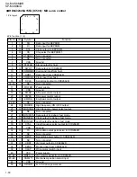
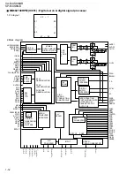
MN101C12GDW (IC851): Panel micon
75
76
100
51
~
~
50
26
~
1
25
~
1.Pin layout
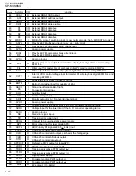
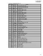
2. Pin function
1
2
3
4~9
10
11
12
13
14
15
16
17~19
20
21
22
23
24
25
26
27~32
33
34
35
36
37~41
42
43
44
45~57
58
59
60
61
62
63
64
65~72
73
74~78
79~86
87~94
95
96
97
98
99
100
Connect to ground.
Input terminal.
Input terminal.
Connect to ground.
A / D Ref. voltage.
Ref. voltage.
OSC frequency input terminal.
OSC frequency output terminal.
Connect to ground.
Connect to ground.
Non use.
Connect to ground.
Connect to ground.
System CPU require signal output terminal.
Stand by LED (RED) output terminal.
Power LED (GREEN) output terminal.
Connect to ground.
Connect to ground.
Panel CPU require signal input terminal.
Connect to ground.
Reset signal input terminal.
Connect to ground.
Connect to ground.
MD (RED) output terminal.
Connect to ground.
Commor signal output terminal.
Commor signal input terminal.
Commor clock signal input terminal.
Connect to ground.
Write enable output terminal.
Read enable output terminal.
Chip select output terminal.
Connect to ground.
Connect to ground.
Data select signal output terminal.
LCD reset signal output terminal.
Connect to ground.
Dimmer control terminal.
Connect to ground.
Pata bus signal output terminal.
Connect to ground.
Connect to ground.
Non use.
Red LED control terminal.
Green LED control terminar.
Blue LED control terminal.
Ref. voltage.
I/O
-
LEVEL Lch
LEVEL Rch
-
A / D Power
Vdd
8.38MHz
8.38MHz
GND
-
-
-
-
comm sysreq
LED STBY red
LED POWER green
-
-
comm panereq
-
comm reset
-
-
LED MD REC
-
comm out
comm in
comm clock
-
LCD WE
LCD RE
LCD CS1
-
-
LCD AO
LCD RESET
-
LCD LEDdimmer
-
LCD D7~D0
-
DVASS
-
LED RED
LED GREEN
LED BLUE
DAVdd
-
I
I
-
-
-
I
O
-
-
-
-
-
O
O
O
-
-
I
-
I
-
-
O
-
O
I
I
-
O
O
O
-
-
O
O
-
O
-
O
-
-
-
O
O
O
-
Pin No.
Symbol
Function

