JK
microsystems
Flashlite 186
User’s Manual
10
Hardware
Jumpers
JP1 - Socket Memory Type / Boot Memory Location
This jumper selects the type of memory in the expansion socket. Available choices are SRAM or
Flash. Other memory types may be supported if their pinout is compatible with standard SRAM
or Flash chips. Jumper pins 1-2 and 3-4 for SRAM or pins 1-3 and 2-4 for Flash. This jumper
also allows the board to boot from the expansion socket. This is useful when performing field
updates of the on-board Flash memory or when using an operating system other than DOS.
Jumper pins 5-7 and 6-8 to boot from the on-board memory or jumper pins 7-9 and 8-10 to boot
from the expansion socket.
Default position:
1-3 and 2-4, Flash memory expansion.
5-7 and 6-8, Boot from on-board flash.
JP2 -Serial Port 0 Select
This jumper selects the drivers and header that will be used for the Serial 0 signals. Serial 0 can
be jumpered as half-duplex RS-485, TTL RS-232 (Rx and Tx), or RS-232 (Rx, Tx, RTS, CTS,
DCD). Install the jumper at location 1-2 for RS-485 signals on J5, 3-4 for TTL RS-232 signals
on J5 or 5-6 for RS-232 signals on J10.
Default position:
5-6, RS-232 Levels on J10.
NOTE: Only 1 jumper may be installed on JP2.
Cables and Connectors
The following tables show the signal name (direction) for each connector pin.
NOTE: N/C indicates no connection and PULLUP indicates a 1k ohm pullup resistor to Vcc.
Outputs are driven by the board and received by a peripheral. Inputs are driven by a
peripheral and received by the board.
Serial 0 is configured as a DTE port, and is generally used to communicate with a peripheral
device. Serial 1 is configured as a DCE port, generally being used to connect the Flashlite to
another computer. Serial Debug is configured as a DCE port, generally being used to connect the
Flashlite to another computer.
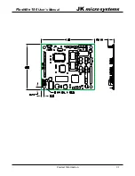
Pin one has a square PCB pad and the others are round. This should be visible on the bottom of
the PCB. Pin one will also be identified on the board silkscreen with a ‘1’ and/or a dot. Dual row
headers have ODD numbered pins on one side and EVEN numbered pins on the other. The dual
row header numbering scheme follows the numbering for an IDC style ribbon cable. This
numbering may not be identical to connectors with discrete wires. Use caution when connecting
cables to the Flashlite.
Summary of Contents for Flashlite 186
Page 1: ...Flashlite 186 User s Manual ...
Page 2: ......
Page 6: ...JKmicrosystems Flashlite 186 User s Manual iv ...
Page 17: ......
Page 27: ...21 Flashlite 186 User s Manual JKmicrosystems Contact Information ...


