


Communication Protocol
109
Node addr.
Command
Data addr.
Read No.
CRC
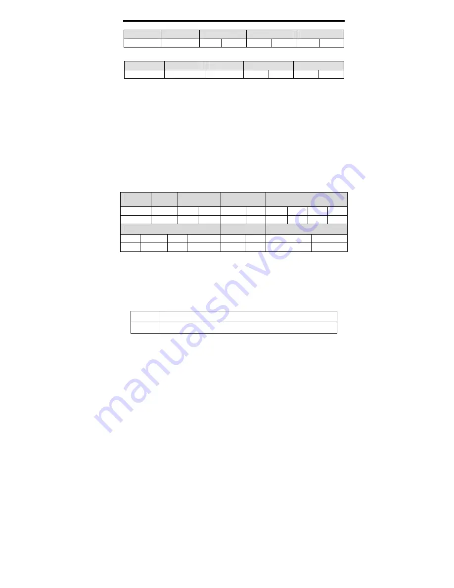
0x01 0x03
0x00
0x02
0x00 0x01 0x25 0xCA
The table below shows the reply frame from slave node address 1
Node addr.
Command
Bytes No.
Data
CRC
0x01 0x03 0x02
0x00 0x00 0xB8
0x44
ASCII mode
In ASCII mode, the frame head is “0x3A”, and default frame tail is “0x0D” or “0x0A”. The
frame tail can also be configured by users. Except frame head and tail, other bytes will be
sent as two ASCII characters, first sending higher nibble and then lower nibble. The data
have 7/8 bits. “A”~“F” corresponds to the ASCII code of respective capital letter. LRC
check is used. LRC is calculated by adding all the successive bytes of the message
except the head and tail, discarding any carriers, and then two’s complementing the
result.
Example of Modbus data frame in ASCII mode:
The command frame of writing 0x0003 into address “0x1000” of slave node address 1 is
shown in the table below:
LRC checksum = the complement of (01+06+10+00+0x00+0x03) = 0xE5
Frame
head
Node addr.
Command
Data addr.
Code 0
1 0 6
1
0
0
0
ASCII 3A 30 31 30 36
31
30
30
30
Data to write
LRC
Frame tail
0 0 0 3 E 5
CR
LF
30 30 30 33 45 35
0D
0A
10.4 Protocol function
Different respond delay can be set through drive’s parameters to adapt to different needs.
For RTU mode, the respond delay should be no less than 3.5 bytes interval, and for
ASCII mode, no less than 1ms.
The main function of Modbus is to read and write parameters. The Modbus protocol
supports the following commands:
0x03
Read inverter’s function parameter and status parameters
0x06
Write single function parameter or command parameter to inverter
All drive’s function parameters, control and status parameters are mapped to Modbus
R/W data address.
The data addresses of each function parameters please refer the sixth column of chapter
9.
Summary of Contents for CHE100-004G-2
Page 7: ......
Page 11: ...Introduction 4 1 4 Parts Description Figure 1 2 Parts of inverters 15kw and below...
Page 20: ...Installation 13 Figure 3 7 Disassembly of metal plate cover Figure 3 8 Open inverter cabinet...
Page 22: ...Wiring 15 4 1 Connection of Peripheral Devices Figure 4 1 Connection of peripheral devices...


