


134
Hardware Design Guide
IXP28XX Network Processor
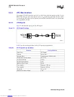
Slowport
7.1.2.1
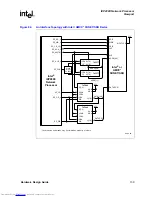
Flash PROM Interface Logic
The following sections describe the address latch logic and provide example implementations of
this logic.
7.1.2.1.1
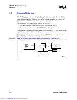
Address Latch Logic
The flash memory interface only supports 8-bit devices; therefore, no data packing or unpacking is
required. Since the address bus is only eight bits wide, the 24-bit address must be latched by the
external logic. The address is shifted out by the network processor, eight bits at a time in three
consecutive clock cycles to form the upper 24 bits (A[25:2]) of the address, while the lower two
bits (A[1:0]) are provided on dedicated pins.
The external logic monitors the SP_ALE_L signal; when this signal is asserted, the external logic
latches the presented address on the SP_AD[7:0] bus on the rising edge of SP_CLK for three
consecutive cycles. The least significant byte (LSB) of the address is delivered first and the most
significant byte (MSB) is presented last.
Note:
Timing diagrams for all supported modes are provided in the Slowport unit section of the
Intel®
IXP2800 Network Processor Hardware Reference Manual
. We recommend that you consult the
HRM and review
all
of the timing diagrams in that section.
The Verilog* code in
Example 1
depicts an example implementation of the logic:
Example 1.
PROM Address Latch Logic
// implementation of address packing logic
always @(posedge sp_clk) begin
if (~rst_l) begin
latched_add <= 24'h000000;
end
else begin
sp_ale_l_d <= sp_ale_l;
if (~sp_ale_l) begin
latched_add[7:0]
<= sp_ad_in;
latched_add[15:8]
<= latched_add[7:0];
latched_add[23:16] <= latched_add[15:8];
end
end // else: !if(~rst_l)
end // always @ (posedge sp_clk)
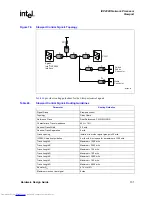
This logic is equivalent to the F377 devices shown in
Figure 81
.
No additional logic is required to interface to the flash.
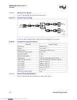
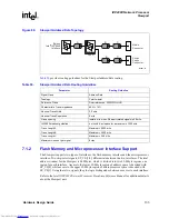
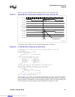
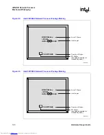
Figure 82
and
Figure 83
depict the timing
for a single write and read transaction, respectively, to the flash memory interface.
Downloaded from
Elcodis.com
electronic components distributor