


Design Guide
44 of 48
V 1.0
2018-06-06
XDPL8218 design guide
For high power factor flyback converter with constant voltage output
Debugging guide
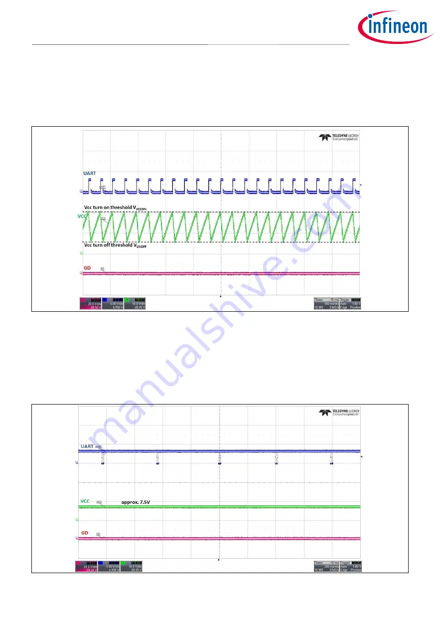
Scenario IV: V
CC
repeatedly hits V
CC
turn-off threshold (6 V typ.) and the GD pin signal always stays low despite
V
CC
recharge to the turn-on threshold (20.5 V typ.). See an example in
This scenario means the configuration mode has likely been entered due to no parameter at start-up. To avoid
this, please burn the first full set of parameters to the XDPL8218 chip.
Figure 29
Scenario IV waveform example (configuration mode entered with no parameter at start-
up)
Scenario V: V
CC
stays constant at approximately 7.5 V and the UART pin signal stays mostly high (see an
example in
This scenario means the configuration mode has been entered due to IC activation by .dp Interface Gen2 before
AC input is applied. To avoid this, disconnect the .dp Interface Gen2 before AC input is applied.
Figure 30
Scenario V waveform (configuration mode entering due to IC activation by .dp Interface
Gen2 voltage supply, before AC input is applied)


