


Design Guide
29 of 48
V 1.0
2018-06-06
XDPL8218 design guide
For high power factor flyback converter with constant voltage output
Regulated mode parameters
The on-time ramp increases from t
on,min
(V
in
) at V
FB,on
, until t
on,max
(V
in
) is reached at V
FB,max,map
.
Note:
t
on,min
(V
in
) and t
on,max
(V
in
) are the on-time limit variables, which are dependent on the estimated
input voltage V
in
. For more details, please refer to
Section 14.2
The switching period ramp increases from 1/f
sw,max
at V
FB,sw
, until 1/f
sw,min
is reached at V
FB,ABM
. When the QR first
valley switching period t
sw,QR1
is above this switching period ramp, QRM1 is entered. When t
sw,QR1
is below this
switching period ramp, DCM is entered.
Note:
f
sw,max
and f
sw,min
are respectively the maximum and minimum switching frequency parameters.
As shown in
, the typical values of V
FB,ABM
, V
FB,on
and V
FB,sw
are fixed as 0.8 V, 1.2 V and 2.0 V, respectively.
Referring to
, the recommended parameter configuration for FB voltage mapping and mode transition
is selected in this design example.
Table 8
Parameter configuration related to FB voltage mapping and mode transition
Parameter name
Recommended value
Unit
V
FB,max,map
2.0
V
V
FB,min
V
CE,sat
(refer to optocoupler
datasheet)
V
t
ABM,blank
6.5
Ms
14.5
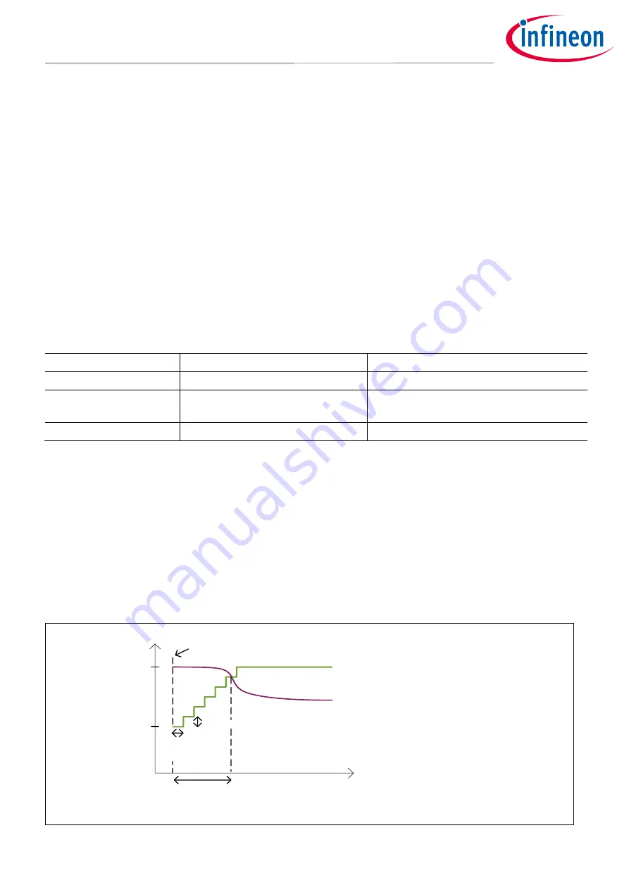
FB voltage maximum limit ramp
Whenever the regulated mode is entered, the filtered FB voltage maximum limit V
FB,filtered,max
is ramped up from
V
FB,limit,start
(1.2 V typ.) to V
REF
(2.428 V typ.), with incremental voltage step based on the V
FB,limit,step
parameter and
time step based on the half sine wave period.
As shown in
, when V
FB,filtered
is higher than V
FB,filtered,max
initially on entering regulated mode, the FB
voltage mapping is based on V
FB,filtered,max
ramp, in order to prevent excessive output rise overshoot. When
V
FB,filtered
gets lower than V
FB,filtered,max
, the FB voltage mapping is then based on V
FB,filtered
.
As a start, V
FB,limit,step
= 800 mV is generally recommended. It can be reduced later after successful powering-up
of the system, if there is excessive output rise overshoot found during the start-up test.
time
Voltage
V
FB,limit,start
V
REF
V
FB,limit,step
Filtered feedback voltage
V
FB,filtered
Filtered feedback voltage max. limit
V
FB,filtered,max
(1.2V typ.)
(2.428V typ.)
Regulated mode entering
Feedback voltage mapping
based on V
FB,filtered,max
(when
V
FB,filtered
> V
FB,filtered,max
)
half sine
wave period
Figure 20
FB voltage maximum limit ramp when entering regulated mode


