Infineon Aurix TC275 Lite Kit 1 Series User Manual Download Page 21

1

1

2

2

3

3

4

4

5

5

6

6

7

7

8

8

D

D

C

C

B

B

A

A

4

4

30.06.2020

15:18:14

Date:

Sheet

of

Time:

© Infineon Technologies AG 2020. All Rights Reserved.

Author:

-

04_CPU.SchDoc

Infineon Technologies AG

Infineon Technologies AG

-

V1.1

Title

Size:

Rev.

A3

Document Name

04_CPU.SchDoc

Rel.

-

Variant

Aurix™ TC275 Lite-Kit

Default_Assembly

Approved

<Appr.>

-

-

SVN Revision:

da75247807cb30a8ab86d75f81b360f14d63d5c9

TRST_N

114

TCK

115

P21_6/TDI

111

P21_7/TDO

113

TMS

112

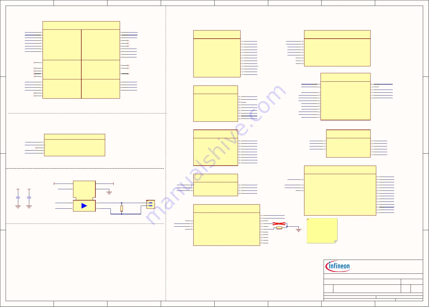
OCDS / JTAG / DAP Control

U6D

AN0

67

AN1

66

AN2

65

AN3

64

AN4

63

AN5

62

AN6

61

AN7

60

AN16

50

AN17

49

AN18

48

AN19

47

AN20

46

AN21

45

AN24/P40_0

44

AN25/P40_1

43

AN26/P40_2

42

AN27/P40_3

41

AN28

40

AN29

39

AN32/P40_4

38

AN33/P40_5

37

AN35

36

AN10

58

AN11

57

AN12

56

AN13

55

AN8

59

AN37/P40_7

34

AN38/P40_8

33

AN39/P40_9

32

AN36/P40_6

35

AN44

31

AN45

30

AN46

29

AN47

28

ADC Groups

Group 0

Analog Inputs

Group 1

Group 2

Group 3/4

Group 5

Group 3/4
Sent/Port 40

U6F

P00_0

11

P00_1

12

P00_2

13

P00_3

14

P00_4

15

P00_5

16

P00_6

17

P00_7

18

P00_8

19

P00_9

20

P00_10

21

P00_11

22

P00_12

23

Port 0

GTM/CCU6/ASC/CAN/VADC

U6G

P02_0

1

P02_1

2

P02_2

3

P02_3

4

P02_4

5

P02_5

6

P02_6

7

P02_7

8

P02_8

9

Port 2

GPIO/GTM/QSPI/CCU6

U6H

P10_0

168

P10_1

169

P10_2

170

P10_3

171

P10_4

172

P10_5

173

P10_6

174

P10_7

175

P10_8

176

Port 10

GPT/GTM/QSPI1

U6I

P11_2

160

P11_3

161

P11_6

162

P11_9

163

P11_10

165

P11_11

166

P11_12

167

Port 11

GTM/QSPI/CCU6

U6J

P13_0

156

P13_1

157

P13_2

158

P13_3

159

P14_0

142

P14_1

143

P14_2

144

P14_3

145

P14_4

146

P14_5

147

P14_6

148

P14_7

149

P14_8

150

P14_9

151

P14_10

152

Port 13 & 14

GTM/I2C0/QSPI2/CAN/CCU6/GPT120

U6K

P15_0

133

P15_1

134

P15_2

135

P15_3

136

P15_4

137

P15_5

138

P15_6

139

P15_7

140

P15_8

141

Port 15

GTM/ASC1/QSPI0,2/CAN2/CCU6/I2C0

U6L

P20_0

116

P20_1

117

P20_3

119

P20_6

124

P20_7

125

P20_8

126

P20_9

127

P20_10

128

P20_11

129

P20_12

130

P20_13

131

P20_14

132

P21_0

105

P21_1

106

P21_2

107

P21_3

108

P21_4

109

P21_5

110

Port 20 & 21

GTM/ASC3/HSCT/QSPI

U6M

P22_0

95

P22_1

96

P22_2

97

P22_3

98

P23_0

89

P23_1

90

P23_2

91

P23_3

92

P23_4

93

P23_5

94

Port 22 & 23

GTM/ASC3/QSPI3

U6N

P32_2

86

P32_3

87

P32_4

88

P33_0

70

P33_2

72

P33_4

74

P33_6

76

P33_8

78

P33_10

80

P33_12

82

P33_1

71

P33_3

73

P33_5

75

P33_7

77

P33_9

79

P33_11

81

P33_13

83

VGATE1N/P32_0

84

Port 32 & 33

ASC/GTM/SENT/QSPI/DSADC/CCU6

U6O

P02.0
P02.1

P02.3
P02.4
P02.5
P02.6
P02.7

RX

MISO
SPICLK
MOSI
P10.4
P10.5

DAP0

DAP1

P21.7

AN39

AN38

AN37

AN36

P14.1

P14.0

/TRST

TX

TX

RX

P00.0
P00.1
P00.2
P00.3

P00.5
P00.6
P00.7

P00.10
P00.11

BUTTON1

LED1
LED2

Potentiometer

AN0

ADC0

ADC1

ADC2

ADC3

ADC4

ADC5

PWM_4

PWM_5

PWM_2

PWM_3

SPICLK

MISO

MOSI

SS0/PWM_10

PWM_9

PWM_8

BDBUS0

BDBUS1

AN44
AN45
AN46
AN47

AN1
AN2
AN3
AN4
AN5
AN6
AN7

P33.0
P33.1
P33.2
P33.3
P33.4
P33.5
P33.6
P33.7
RXD1_S2G1
TXD1_S2G1
P33.10
P33.11
P33.12
P33.13

P32.0

P23.0
P23.1
P23.2
P23.3
P23.4
P23.5

P22.0
P22.1
P22.2

TXD2_S2G2
P20.1

RXD2_S2G2

P15.4
P15.5

P11.3

Analog Circuit of AURIX TC275

DAP Control of AURIX TC275

Ports of AURIX TC275

#CANH

#CANL

#CAN_RXD
#CAN_TXD

C46
100nF

C47
100nF

GND

GND

#NEN

CAN Tranceiver

ADC5/SCL0

ADC4/SDA0

SDA0/AN24

SCL0/AN25

TXD0_MB
RXD0_MB

TX Mikrobus

RX Mikrobus

SS_MB

SS Mikrobus

RST_MB

Reset Mikrobus

PWM_MB

PWM Mikrobus

INT_MB

Interrupt Mikrobus

ADC Mikrobus

AN1_S2G1

AN1_S2G2

AN2_S2G1

AN2_S2G2

GND

PWM_S2G1
PWM_S2G2

P21.0

P21.2
P21.3
P21.4
P21.5

RST_S2G1
RST_S2G2

GPIO1_S2G1
GPIO1_S2G2

P00.8
P00.9

P20.10

P20.14

SDA0/AN24
SCL0/AN25
AN26_MB

1
2

CAN

HTSW-102-07-L-S

R15
120R

CS_S2G1

CS_S2G2

INT_S2G1

INT_S2G2

P00.12

P11.6

+5V

P22.3

SCLK

P11.11

P11.9

P11.12

PWM_6

PWM_7

R30

1k

R31

1k

TXD

1

GND

2

RXD

4

CANL

6

CANH

7

STB

8

VCC

3

VIO

5

U7

TLE9251VSJ

+5V

VEXT

VEXT

#NEN

#CAN_TXD

#CAN_RXD

GND

MTSR

SS

MRST

MDC

MDIO

-Resistor (R31) at P14.3 
can be assembled 
manually. But then 
overboots P10.5/P10.6

-Resistor (R30) at P14.5 is 
mandatory

Summary of Contents for Aurix TC275 Lite Kit 1 Series

Page 1: ...Microcontroller Evaluation Board For Aurix TC275 Board User s Manual Revision 01 June 2020 Aurix TC275 Lite Kit Kit Version 1 1...

Page 2: ...ery terms and conditions and prices please contact the nearest Infineon Technologies Office www infineon com Warnings Due to technical requirements components may contain dangerous substances For info...

Page 3: ...ed by FlexRay Consortium HYPERTERMINAL of Hilgraeve Incorporated IEC of Commission Electrotechnique Internationale IrDA of Infrared Data Association Corporation ISO of INTERNATIONAL ORGANIZATION FOR S...

Page 4: ...14 4 1 USB Connector 14 4 2 Serial Connection to PC 14 4 3 Bootmode 14 4 4 Config Signals 15 4 5 Infineon DAP Debug Connector 10 pin 15 4 6 miniWiggler JDS 16 5 Reset 16 5 1 CAN Transceiver 16 5 2 Sch...

Page 5: ...e 2 Signal mapping of the 0 Ohm Pin Bridges 12 Table 3 Aurix Pin Mapping for User LEDs 13 Table 4 Debugger Pin Mapping for User LEDs 14 Table 5 Aurix Push Buttons and Potentiometer 14 Table 6 User Sta...

Page 6: ...overview specifications of the whole board Table 1 Overview of the Board Specification CPU Core Aurix Manufacturer Order No SAK TC275TP 64F200W DB Type TC1 6P TC1 6E P Cores Checker Cores E Cores Chec...

Page 7: ...PC is within 64 bytes of the top of an instruction memory the Instruction Fetch Unit may attempt to speculatively fetch instruction from beyond the physical range This may then lead to error conditio...

Page 8: ...n deliver up to 500 mA current and USB3 0 up to 900mA For best performance we recommend to use USB3 0 If higher currents are required and in order to avoid damages on the USB host the use of an extern...

Page 9: ...dering the resitstor R27 size 0805 imp you can use an external 3V3 source on either one of the VEXT pins at X1 X2 connectors or the 3V3 pin on the X302 Arduino power connector to power the board Note...

Page 10: ...2 P00 8 9 10 P00 7 Button1 P23 5 11 12 P23 4 P00 10 11 12 P00 9 MRST P22 1 13 14 P22 0 MTSR P00 12 13 14 P00 11 P21 0 15 16 P22 2 SS VAREF1 15 16 AN47 MDC P21 2 17 18 P22 3 SCLK AN46 17 18 AN45 P21 4...

Page 11: ...IO1 P32 2 13 5 13 12 SCL GPIO1 P32 3 13 6 GND GND CS P11 2 14 6 GND GND CS P11 10 14 7 VEXT 3V3 SCLK P10 21 15 7 VEXT 3V3 SLCK P10 21 15 8 P00 4 INT GPIO3 MOSI P10 31 16 8 P10 8 INT GPIO3 MOSI P10 31...

Page 12: ...ix 0402 Assemble if needed but overboots then P10 5 P10 6 R37 0 yes XTAL2 Aurix 0805 Serial resistor to reduce oscillator aplitude if needed R39_opt 0 no USR0 ADBUS6 Debug 1210 Placeholder do not asse...

Page 13: ...el operation of I2C and ADC4 ADC5 is not possible because they share the same pins at the Arduino connector X301 and X303 3 4 User Push Buttons User LEDs and Potentiometer The Aurix TC275 Lite Kit pro...

Page 14: ...r connection to a PC Via the USB it is possible to power the board using the ASCLIN0 as serial connection via USB and Debugging via DAS NOTE Before connecting the board to the PC make sure that the ac...

Page 15: ...ou use this connector make sure that the miniWiggler JDS is not activ LED D2 is off For more information we refer you to the DAP Connector Manual Table 8 Pin Assignment of the DAP Debug Connector Pin...

Page 16: ...er depending on the used debugger client IMPORTANT Make sure that there is no or a tristated connection on the DAP connector if the LED D1 is on 5 Reset The power on reset input pin PORST of the Aurix...

Page 17: ...l 17 Revision June 2020 Table 9 CAN Signals and Aurix TC275 Pin Mapping Signal Name Pin No at CAN Pin Header Aurix Pin Aurix Function Ass Reg I O Line CANH 1 CANL 2 CAN_TX P20 8 CAN node 0 output TXDC...

Page 18: ...G THE INFORMATION GIVEN IN THIS DOCUMENT IS GIVEN FOR ILLUSTRATING PURPOSES ONLY THE RECIPIENT OF THIS DOCUMENT MUST VERIFY ANY FUNCTION DESCRIBED HEREIN IN THE REAL APPLICATION INFINEON TECHNOLOGIES...

Page 19: ...PIIC103 PIIC104 PIIC105 PIIC106 PIIC107 PIIC108 PIIC109 PIIC1010 PIIC1011 PIIC1012 PIIC1013 PIIC1014 PIIC1015 PIIC1016 PIIC1017 PIIC1018 PIIC1019 PIIC1020 PIIC1021 PIIC1022 PIIC1023 PIIC1024 PIIC1025...

Page 20: ...2 PIQ203 COQ2 PIR1001 PIR1002 COR10 PIR1301 PIR1302 COR13 PIR2001 PIR2002 COR20 PIR2101 PIR2102 COR21 PIR2201 PIR2202 COR22 PIR2301 PIR2302 COR23 PIR2401 PIR2402 COR24 PIR2501 PIR2502 COR25 PIR2601 PI...

Page 21: ...ory PIC4601 PIC4602 COC46 PIC4701 PIC4702 COC47 PICAN01 PICAN02 COCAN PIR1501 PIR1502 COR15 PIR3001 PIR3002 COR30 PIR3101 PIR3102 COR31 PIU60111 PIU60112 PIU60113 PIU60114 PIU60115 COU6D PIU6028 PIU60...

Page 22: ...eramic Capacitor 0402YD104KAT2A YES TOP 6 4 C9 C22 C45 C100 100nF Surface Mount Multilayer Ceramic Chip Capacitor C0402C104K9RACTU C0402T104K4RACTU YES TOP 7 1 C10 100nF Surface Mount Multilayer Ceram...

Page 23: ...tandard Thick Film Chip Resistor CRCW040210K0FK YES TOP 28 2 R4 R5 22R Standard Thick Film Chip Resistor CRCW040222R0FK YES TOP 29 3 R6 R30 R36 1k 1k 50V 5 RC0402JR 131KL YES TOP 30 1 R7 12k Standard...

Page 24: ...Type AB Bottom Mount Shell SMT ZX62 AB 5PA 31 YES TOP 50 1 X300 Through hole 025 SQ Post Header 2 54mm pitch 6 pin vertical double row female TSW 103 07 L D NO TOP 51 1 X301 Through hole 025 SQ Post H...

Page 25: ...w w w i n f i n e o n c o m Published by Infineon Technologies AG...

Reviews: