background image


WAFER-PV-D5252/D4252/N4552 SBC 

Page 3

1.3 Features 

Some of the WAFER-PV-D5252/D4252/N4552 motherboard features are listed below: 

ƒ


3.5" form factor 

ƒ

 Fanless 

design 


ƒ

 RoHS 

compliant 

ƒ


Eight USB 2.0 ports 

ƒ


Six serial ports   

ƒ


PCIe Mini card slot 

ƒ


CompactFlash® Type II slot 

ƒ

 Gigabit 

Ethernet 

1.4 Connectors 

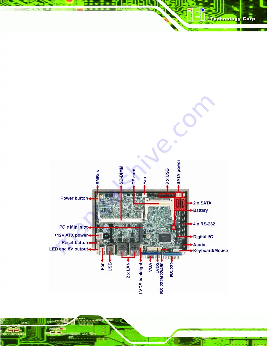
The connectors on the WAFER-PV-D5252/D4252/N4552 are shown in the figure below. 

Figure 1-2: Connectors 

Summary of Contents for WAFER-PV-D5252

Page 1: ...2 SBC Page i IEI Technology Corp User Manual WAFER PV D5252 D4252 N4552 MODEL 3 5 SBC with Intel Atom Processor Up to 2 0 GB DDR3 VGA LVDS PCIe Mini RS 232 422 485 SATA 3Gb s CompactFlash Eight USB Ro...

Page 2: ...Date Version Changes 20 March 2013 1 02 Modified supported memory specifications Table 1 1 4 March 2011 1 01 Modified LVDS connector pinouts Table 3 11 Modified LVDS resolution select jumper settings...

Page 3: ...mages arising out of the use or inability to use the product or documentation even if advised of the possibility of such damages This document contains proprietary information protected by copyright A...

Page 4: ...L ITEMS 12 3 CONNECTOR PINOUTS 13 3 1 PERIPHERAL INTERFACE CONNECTORS 14 3 1 1 Layout 14 3 1 2 Peripheral Interface Connectors 15 3 1 3 External Interface Panel Connectors 16 3 2 INTERNAL PERIPHERAL C...

Page 5: ...et Connectors 35 3 3 2 Serial Port Connector 36 3 3 3 USB Ports 37 3 3 4 VGA Connector 37 4 INSTALLATION 39 4 1 ANTI STATIC PRECAUTIONS 40 4 2 INSTALLATION CONSIDERATIONS 41 4 3 SO DIMM INSTALLATION 4...

Page 6: ...ON 64 5 1 1 Starting Setup 64 5 1 2 Using Setup 64 5 1 3 Getting Help 65 5 1 4 Unable to Reboot After Configuration Changes 65 5 1 5 BIOS Menu Bar 65 5 2 MAIN 66 5 3 ADVANCED 67 5 3 1 ACPI Configurati...

Page 7: ...Build up Recovery Partition 103 B 2 5 Create Factory Default Image 105 B 3 SETUP PROCEDURE FOR LINUX 110 B 4 RECOVERY TOOL FUNCTIONS 113 B 4 1 Factory Restore 115 B 4 2 Backup System 116 B 4 3 Restor...

Page 8: ...22 Figure 3 9 LED and 5 V Power Output Connector Location 23 Figure 3 10 LVDS Connector Location 24 Figure 3 11 Backlight Inverter Connector 25 Figure 3 12 PCIe Mini Card Slot Location 26 Figure 3 13...

Page 9: ...54 Figure 4 13 Keyboard mouse Y cable Connection 55 Figure 4 14 Four Serial Port Connector 56 Figure 4 15 Serial Device Connector 57 Figure 4 16 LAN Connection 58 Figure 4 17 Serial Device Connector...

Page 10: ...09 Figure B 21 Press Any Key to Continue 110 Figure B 22 Partitions for Linux 111 Figure B 23 System Configuration for Linux 112 Figure B 24 Access menu lst in Linux Text Mode 112 Figure B 25 Recovery...

Page 11: ...put Connector Pinouts 23 Table 3 11 LVDS Connector Pinouts 24 Table 3 12 Backlight Inverter Connector 25 Table 3 13 PCIe Mini Card Slot Pinouts 27 Table 3 14 Power Button Connector Pinouts 27 Table 3...

Page 12: ...45 Table 4 3 Clear CMOS Jumper Settings 46 Table 4 4 LVDS Voltage Selection 47 Table 4 5 LVDS Resolution Selection 47 Table 4 6 CompactFlash Master Slave Selection 48 Table 4 7 COM3 RS 232 422 485 Sel...

Page 13: ...nu 7 Super IO Configuration 72 BIOS Menu 8 Serial Port n Configuration Menu 73 BIOS Menu 9 Hardware Health Configuration 78 BIOS Menu 10 Serial Port Console Redirection 80 BIOS Menu 11 Chipset 81 BIOS...

Page 14: ...WAFER PV D5252 D4252 N4552 SBC Page 1 Chapter 1 1 Introduction...

Page 15: ...s handled by a SATA 3Gb s port for connecting a hard drive optical drive or SSD The CompactFlash slot allows a Type II CompactFlash card to be installed The board has two graphics outputs A VGA output...

Page 16: ...rboard features are listed below 3 5 form factor Fanless design RoHS compliant Eight USB 2 0 ports Six serial ports PCIe Mini card slot CompactFlash Type II slot Gigabit Ethernet 1 4 Connectors The co...

Page 17: ...WAFER PV D5252 D4252 N4552 SBC Page 4 1 5 Dimensions The main dimensions of the WAFER PV D5252 D4252 N4552 are shown in the diagram below Figure 1 3 Dimensions without Heatsink mm...

Page 18: ...WAFER PV D5252 D4252 N4552 SBC Page 5 Figure 1 4 Dimensions with Heatsink mm...

Page 19: ...WAFER PV D5252 D4252 N4552 SBC Page 6 1 6 Data Flow Figure 1 5 shows the data flow between the system chipset the CPU and other components installed on the motherboard Figure 1 5 Data Flow Diagram...

Page 20: ...DDR3 SDRAM SO DIMM D525 D425 system max 4 0 GB N455 system max 2 0 GB Graphic Engine Intel GMA3150 D525 D425 Gen 3 5 DX9 400 MHz N455 Gen 3 5 DX9 200 MHz Integrated Graphics Analog CRT CRT hot plug s...

Page 21: ...slot SATA Two independent SATA channels with 3 0 Gb s data transfer rates Environmental and Power Specifications Power Supply AT or ATX 12 V only Power Consumption 12 V 1 79 A 1 8 GHz Intel Atom D525...

Page 22: ...WAFER PV D5252 D4252 N4552 SBC Page 9 Chapter 2 2 Packing List...

Page 23: ...charge Self grounding Touch a grounded conductor every few minutes to discharge any excess static buildup Use an anti static pad When configuring any circuit board place it on an anti static mat Only...

Page 24: ...rom or contact an IEI sales representative directly by sending an email to sales iei com tw The WAFER PV D5252 D4252 N4552 is shipped with the following components Quantity Item and Part Number Image...

Page 25: ...ack 2 0mm P N 33100 000033 RS 1 Utility CD 1 Quick installation guide Table 2 1 Packing List 2 4 Optional Items These optional items are available Item and Part Number Image Dual USB cable wo bracket...

Page 26: ...WAFER PV D5252 D4252 N4552 SBC Page 13 Chapter 3 3 Connector Pinouts...

Page 27: ...ws peripheral interface connector locations Section 3 1 2 lists all the peripheral interface connectors seen in Section 3 1 2 3 1 1 Layout The figure below shows the on board peripheral connectors rea...

Page 28: ...1 Fan connectors 3 pin wafer FAN1 FAN2 Keyboard mouse connector 6 pin wafer KB MS1 LED indicators and 5 V power output connector 6 pin wafer CN2 LVDS connector 30 pin crimp LVDS1 LVDS backlight connec...

Page 29: ...port connector DB 9 COM1 VGA connector 15 pin female VGA VGA1 Table 3 2 Rear Panel Connectors 3 2 Internal Peripheral Connectors Internal peripheral connectors are found on the motherboard and are on...

Page 30: ...3 ATX Power Connector Pinouts 3 2 2 Audio Connector CN Label AUDIO1 CN Type 10 pin header CN Location See Figure 3 3 CN Pinouts See Table 3 4 This connector connects to speakers a microphone and an a...

Page 31: ...ocation See Figure 3 4 CN Pinouts See Table 3 5 This is connected to the system battery The battery provides power to the system clock to retain the time when power is turned off Figure 3 4 Battery Co...

Page 32: ...CF CF must be set to slave A CompactFlash Type I or Type II card can be used in this slot Figure 3 5 CompactFlash Slot Location Pin Description Pin Description 1 GND 26 CD1 2 D3 27 D11 3 D4 28 D12 4 D...

Page 33: ...D1 47 D8 23 D2 48 D9 24 IOCS16 49 D10 25 CD2 50 GND2 Table 3 6 CompactFlash Slot Pinouts 3 2 5 Digital I O Connector CN Label DIO1 CN Type 10 pin header CN Location See Figure 3 6 CN Pinouts See Table...

Page 34: ...8 Input 2 9 Input 1 10 Input 0 Table 3 7 Digital I O Connector Pinouts 3 2 6 Fan Connectors CN Label FAN1 FAN2 CN Type 3 pin wafer CN Location See Figure 3 7 CN Pinouts See Table 3 8 The fan connecto...

Page 35: ...mouse connector connects to a PS 2 Y cable that can be connected to a PS 2 keyboard and mouse Figure 3 8 Keyboard Mouse Connector Location Pin Description 1 VCC 2 Mouse Data 3 Mouse Clock 4 Keyboard D...

Page 36: ...d via this connector Figure 3 9 LED and 5 V Power Output Connector Location Pin Description 1 5 V 5 V Power Output 2 GND 3 VCC Power LED 4 GND 5 VCC HDD LED 6 HDLED Table 3 10 LED and 5 V Power Output...

Page 37: ...A_Y0 5 A_Y1 6 A_Y1 7 A_Y2 8 A_Y2 9 A_CK 10 A_CK 11 NC 12 NC 13 GND3 14 GND4 15 NC 16 NC 17 NC 18 NC 19 NC 20 NC 21 NC 22 NC 23 NC 24 NC 25 GND5 26 GND6 27 VCC_LCD 28 VCC_LCD 29 VCC_LCD 30 VCC_LCD Tab...

Page 38: ...OUND 3 12V 4 GROUND 5 BACKLIGHT ENABLE Table 3 12 Backlight Inverter Connector 3 2 11 PCIe Mini Card Slot CN Label CN1 CN Type PCIe Mini card slot CN Location See Figure 3 12 CN Pinouts See Table 3 13...

Page 39: ...7 CLKREQ 8 LFRAME 9 GND 10 LAD3 11 CLK 12 LAD2 13 CLK 14 LAD1 15 GND 16 LAD0 17 PCIRST 18 GND 19 LPC 20 VCC3 21 GND 22 PCIRST 23 PERN2 24 3VDual 25 PERP2 26 GND 27 GND 28 1 5V 29 GND 30 SMBCLK 31 PET...

Page 40: ...e 2 pin wafer CN Location See Figure 3 13 CN Pinouts See Table 3 14 The power button connector is connected to a power switch on the system chassis Figure 3 13 Power Button Connector Location Pin Desc...

Page 41: ...ctor Location Pin Description 1 PM_RESET 2 GND Table 3 15 Reset Button Connector Pinouts 3 2 14 RS 232 422 485 Serial Port Connector COM2 CN Label COM2 CN Type 14 pin header CN Location See Figure 3 1...

Page 42: ...22 485 Serial Port Connector Pinouts 3 2 15 RS 232 Serial Port Connector COM3 COM6 CN Label COM CN Type 40 pin header CN Location See Figure 3 16 CN Pinouts See Table 3 17 This connector provides RS 2...

Page 43: ...MIT DATA TXD5 26 CLEAR TO SEND CTS5 27 DATA TERMINAL READY DTR5 28 RING INDICATOR RI5 29 GND 30 GND 31 DATA CARRIER DETECT DCD6 32 DATA SET READY DSR6 33 RECEIVE DATA RXD6 34 REQUEST TO SEND RTS6 35 T...

Page 44: ...Pinouts 3 2 17 SATA Power Connectors CN Label SATA_PWR1 SATA_PWR2 CN Type 2 pin wafer CN Location See Figure 3 18 CN Pinouts See Table 3 19 Use the SATA Power Connector to connect to SATA device power...

Page 45: ...m Management Bus connector provides low speed system management communications Figure 3 19 SMBus Connector Location Pin Description 1 GND 2 SMBDATA 3 SMBCLK 4 5V Table 3 20 SMBus Connector Pinouts 3 2...

Page 46: ...CN Label JSPI1 CN Type 8 pin header CN Location See Figure 3 21 CN Pinouts See Table 3 21 The 8 pin SPI Flash connector is used to flash the BIOS Figure 3 21 SPI Flash Connector Location Pin Descript...

Page 47: ...SB4 CN Type 8 pin header CN Location See Figure 3 22 CN Pinouts See Table 3 22 The USB header can connect to two USB devices Figure 3 22 USB Connector Location Pin Description Pin Description 1 VCC 2...

Page 48: ...ernal interface connectors are shown in Figure 3 23 Figure 3 23 External Interface Connectors 3 3 1 Ethernet Connectors CN Label LAN1 LAN2 CN Type RJ 45 CN Location See Figure 3 23 CN Pinouts See Tabl...

Page 49: ...ESCRIPTION OFF 10Mbps connection OFF No link GREEN 100Mbps connection YELLOW Linked ORANGE 1Gbps connection BLINKING Data Activity Table 3 24 RJ 45 Ethernet Connector LEDs 3 3 2 Serial Port Connector...

Page 50: ...ion See Figure 3 23 CN Pinouts See Table 3 26 The USB ports attach to standard USB devices Pin Description 1 VCC 2 Data1 3 Data1 4 Ground 5 VCC 6 Data2 7 Data2 8 Ground Table 3 26 USB Connector Pinout...

Page 51: ...GA connector connects to a CRT or LCD monitor Pin Description Pin Description Pin Description 1 RED 6 GROUND 11 NC 2 GREEN 7 GROUND 12 SDA 3 BLUE 8 GROUND 13 HSYNC 4 5V 9 NC 14 VSYNC 5 GROUND 10 GROUN...

Page 52: ...WAFER PV D5252 D4252 N4552 SBC Page 39 Chapter 4 4 Installation...

Page 53: ...ns whenever the WAFER PV D5252 D4252 N4552 or any other electrical component is handled Wear an anti static wristband Wearing a simple anti static wristband can help to prevent ESD from damaging the b...

Page 54: ...y followed in order to prevent damage to the WAFER PV D5252 D4252 N4552 WAFER PV D5252 D4252 N4552 components and injury to the user Before and during the installation please DO the following Read the...

Page 55: ...me in contact with the PCB circuit connector pins or its components 4 3 SO DIMM Installation To install an SO DIMM please follow the steps below and refer to Figure 4 1 Figure 4 1 SO DIMM Installation...

Page 56: ...1 Locate the CF card socket Locate the CompactFlash slot Step 2 Align the CF card Align the CompactFlash card The label side should be facing away from the board The grooves on the CompactFlash slot...

Page 57: ...AFER PV D5252 D4252 N4552 is installed in the system the jumpers must be set in accordance with the desired configuration The jumpers on the WAFER PV D5252 D4252 N4552 are listed in Table 4 1 Descript...

Page 58: ...th jumpers should be the same Pin Description Short 1 2 ATX mode Default Short 2 3 AT mode Table 4 2 AT ATX Mode Selection Figure 4 3 AT ATX Mode Selection Jumper Location 4 5 2 Clear CMOS Jumper Jump...

Page 59: ...Failsafe Defaults After having done one of the above save the changes and exit the CMOS Setup menu The clear CMOS jumper settings are shown in Table 4 3 Pin Description 1 2 Keep CMOS Setup Default 2 3...

Page 60: ...8 pin header Jumper Settings See Table 4 5 Jumper Location See Figure 4 6 Selects the resolution of the LCD panel connected to the LVDS1 connector Pin Description Open 640 x 480 18 bit Short 1 2 800...

Page 61: ...election Jumper Label JCF1 Jumper Type 2 pin header Jumper Settings See Table 4 6 Jumper Location See Figure 4 7 NOTE To use SATA and CF CF must be set as slave Sets the CompactFlash slot as the IDE p...

Page 62: ...P1 Jumper Type 8 pin header Jumper Settings See Table 4 7 Jumper Location See Figure 4 8 Selects the communication method of COM2 serial port Pin Description Short 1 2 RS 232 Default Short 3 4 RS 422...

Page 63: ...9 Setting jumper configures pin 9 on COM 1 as either a 5 V 12 V power source or as a ring in RI line The COM 1 Pin 9 Setting jumper selection options are shown in Table 4 8 Setting Description Short...

Page 64: ...the cooling fan of a power supply can also help generate airflow through the board surface 4 6 2 Motherboard Installation To install the WAFER PV D5252 D4252 N4552 motherboard into the chassis please...

Page 65: ...ble to Power Supply Connect one of the 4 pin 1x4 Molex type power cable connectors to an AT power supply See Figure 4 12 4 7 2 Audio Kit Installation The Audio Kit that came with the WAFER PV D5252 D4...

Page 66: ...on the on board connector with pin 1 on the audio kit connector Pin 1 on the audio kit connector is indicated with a white dot See Figure 4 11 Figure 4 11 Audio Kit Cable Connection Step 3 Connect the...

Page 67: ...e WAFER PV D5252 D4252 N4552 and branches into two cables that are each connected to a PS 2 connector one for a mouse and one for a keyboard To connect the keyboard mouse Y cable connector please foll...

Page 68: ...tors to the chassis The keyboard mouse Y cable connector is connected to two PS 2 connectors To secure the PS 2 connectors to the chassis please refer to the installation instructions that came with t...

Page 69: ...Step 1 Locate the COM connector The locations of the COM port connectors are shown in Chapter 4 Step 2 Insert the cable connector Align the cable connector with the onboard connector Make sure pin 1...

Page 70: ...ection Single Connector There are two external RJ 45 LAN connectors The RJ 45 connectors enable connection to an external network To connect a LAN cable with an RJ 45 connector please follow the instr...

Page 71: ...PV D5252 D4252 N4552 has a single female DB 9 connector on the external peripheral interface panel for a serial device Follow the steps below to connect a serial device to the WAFER PV D5252 D4252 N45...

Page 72: ...The external USB Series A receptacle connectors provide easier and quicker access to external USB devices Follow the steps below to connect USB devices to the WAFER PV D5252 D4252 N4552 Step 1 Locate...

Page 73: ...N4552 please follow the instructions below Step 1 Locate the female DB 15 connector The location of the female DB 15 connector is shown in Chapter 3 Step 2 Align the VGA connector Align the male DB 1...

Page 74: ...er side of the connector Step 0 4 9 Software Installation All the drivers for the WAFER PV D5252 D4252 N4552 are on the CD that came with the system To install the drivers please follow the steps belo...

Page 75: ...igure 4 20 Introduction Screen Step 3 Click WAFER PV D5252 D4252 N4552 Step 4 A new screen with a list of available drivers appears Figure 4 21 Figure 4 21 Available Drivers Step 5 Install all of the...

Page 76: ...WAFER PV D5252 D4252 N4552 SBC Page 63 Chapter 5 5 BIOS...

Page 77: ...UP message appears on the screen 0 If the message disappears before the F2 key is pressed restart the computer and try again 5 1 2 Using Setup Use the arrow keys to highlight items press ENTER to sele...

Page 78: ...the Help Window press ESC or the F1 key again 5 1 4 Unable to Reboot After Configuration Changes If the computer cannot boot after changes to the system configuration is made CMOS defaults Use the jum...

Page 79: ...the Time Use Tab to switch between Time elements Select Screen Select Item EnterSelect F1 General Help F2 Previous Values F3 Optimized Defaults F4 Save ESC Exit Version 2 02 1205 Copyright C 2010 Ame...

Page 80: ...le with the hardware Aptio Setup Utility Copyright C 2010 American Megatrends Inc Main Advanced Chipset Boot Security Save Exit ACPI Settings CPU Configuration IDE Configuration USB Configuration Supe...

Page 81: ...n 2 02 1205 Copyright C 2010 American Megatrends Inc BIOS Menu 3 ACPI Configuration ACPI Sleep State S1 CPU Stop Clock Use the ACPI Sleep State option to specify the sleep state the system enters when...

Page 82: ...1 General Help F2 Previous Values F3 Optimized Defaults F4 Save ESC Exit Version 2 02 1205 Copyright C 2010 American Megatrends Inc BIOS Menu 4 CPU Configuration The CPU Configuration menu BIOS Menu 4...

Page 83: ...eral Help F2 Previous Values F3 Optimized Defaults F4 Save ESC Exit Version 2 02 1205 Copyright C 2010 American Megatrends Inc BIOS Menu 5 IDE Configuration ATA IDE Configurations Enhanced Use the ATA...

Page 84: ...oard 2 Hubs Legacy USB Support Enabled Enables Legacy USB support AUTO option disables legacy support if no USB devices are connected DISABLE option will keep USB devices available only for EFI applic...

Page 85: ...e the Super IO Configuration menu BIOS Menu 7 to set or change the configurations for the FDD controllers parallel ports and serial ports Aptio Setup Utility Copyright C 2010 American Megatrends Inc A...

Page 86: ...s F3 Optimized Defaults F4 Save ESC Exit Version 2 01 1204 Copyright C 2010 American Megatrends Inc BIOS Menu 8 Serial Port n Configuration Menu 5 3 5 1 1 Serial Port 0 Configuration Serial Port Enabl...

Page 87: ...ettings Auto Use the Change Settings option to change the serial port IO port address and interrupt address Auto DEFAULT The serial port IO port address and interrupt address are automatically detecte...

Page 88: ...IRQ 10 11 Serial Port I O port address is 3E8h and the interrupt address is IRQ10 11 IO 2E8h IRQ 10 11 Serial Port I O port address is 2E8h and the interrupt address is IRQ10 11 5 3 5 1 4 Serial Port...

Page 89: ...on to enable or disable the serial port Disabled Disable the serial port Enabled DEFAULT Enable the serial port Change Settings Auto Use the Change Settings option to change the serial port IO port ad...

Page 90: ...the Change Settings option to change the serial port IO port address and interrupt address Auto DEFAULT The serial port IO port address and interrupt address are automatically detected IO 2C8h IRQ 10...

Page 91: ...emperature Bound 1 60 Temperature Bound 2 50 Temperature Bound 3 40 Temperature Bound 4 30 SYS Smart Fan control Auto Mode Temperature Bound 1 60 Temperature Bound 2 50 Temperature Bound 3 40 Temperat...

Page 92: ...settings Temperature Bound 1 Temperature Bound 2 Temperature Bound 3 Temperature Bound 4 Manual Mode The fan spins at the speed set in Manual Duty Cycle Setting 5 3 7 Serial Port Console Redirection...

Page 93: ...ction Disabled Console Redirection Settings COM5 Console Redirection Disabled Console Redirection Settings Console Redirection Enable Disable Select Screen Select Item EnterSelect F1 General Help F2 P...

Page 94: ...pset BIOS menu may cause the system to malfunction Aptio Setup Utility Copyright C 2010 American Megatrends Inc Main Advanced Chipset Boot Security Save Exit Host Bridge South Bridge Intel IGD SWSCI O...

Page 95: ...atrends Inc Chipset OnChip VGA Configuration Memory Information Memory Frequency 800 Mhz Total Memory 2048 MB DIMM 0 2048 MB DIMM 1 Not present Config On Chip VGA Settings Select Screen Select Item En...

Page 96: ...imized Defaults F4 Save ESC Exit Version 2 01 1204 Copyright C 2010 American Megatrends Inc BIOS Menu 13 OnChip VGA Configuration Share Memory Size 8 MB Use the Share Memory Size option to set the amo...

Page 97: ...zalia HD Audio Select Screen Select Item EnterSelect F1 General Help F2 Previous Values F3 Optimized Defaults F4 Save ESC Exit Version 2 02 1205 Copyright C 2010 American Megatrends Inc BIOS Menu 14 S...

Page 98: ...t enabled USB 2 0 EHCI Support Enabled Use the USB 2 0 EHCI Support BIOS option to enable or disable the USB 2 0 controller Enabled DEFAULT USB 2 0 controller enabled Disabled USB 2 0 controller disab...

Page 99: ...Intel IGD SWSCI OpRegion DVMT Mode Select DVMT Mode Use the DVMT Mode Select option to select the Intel Dynamic Video Memory Technology DVMT operating mode Fixed Mode A fixed portion of graphics memo...

Page 100: ...t 1280x800 18bit 1280x600 18bit 5 5 Boot Use the Boot menu BIOS Menu 16 to configure system boot options Aptio Setup Utility Copyright C 2010 American Megatrends Inc Main Advanced Chipset Boot Securit...

Page 101: ...it Off Does not enable the keyboard Number Lock automatically To use the 10 keys on the keyboard press the Number Lock key located on the upper left hand corner of the 10 key pad The Number Lock LED o...

Page 102: ...boot or enter Setup In Setup the User will have Administrator rights Administrator Password User Password Set User Password Set Master Password Set Setup Administrator Password Select Screen Select I...

Page 103: ...anges and Reset Use the Save Changes and Reset option to save the changes made to the BIOS options and to exit the BIOS configuration setup program Discard Changes and Reset Use the Discard Changes an...

Page 104: ...WAFER PV D5252 D4252 N4552 SBC Page 91 Appendix A A BIOS Options...

Page 105: ...s Auto 74 Serial Port Enabled 74 Change Settings Auto 75 Serial Port Enabled 75 Change Settings Auto 75 Serial Port Enabled 76 Change Settings Auto 76 Serial Port Enabled 77 Change Settings Auto 77 PC...

Page 106: ...S Default 87 Bootup NumLock State On 88 Quiet Boot Enabled 88 Launch PXE OpROM Disabled 88 Administrator Password 89 User Password 89 Save Changes and Reset 90 Discard Changes and Reset 90 Restore Def...

Page 107: ...WAFER PV D5252 D4252 N4552 SBC Page 94 Appendix B B One Key Recovery...

Page 108: ...ool as shown in 77Figure B 1 to backup or restore Windows system five setup procedures are required 1 Hardware and BIOS setup see Section 77B 2 1 2 Create partitions see Section 77B 2 2 3 Install oper...

Page 109: ...or the operating system while the second partition will be invisible to the operating system and contain the backup made by the one key recovery software The partition created for recovery images must...

Page 110: ...ported OS versions are listed below Microsoft Windows o Windows XP Service Pack 2 or 3 required o Windows Vista o Windows 7 o Windows CE 5 0 o Windows CE 6 0 o Windows XP Embedded Linux o Fedora Core...

Page 111: ...partition see Section 77B 2 4 Step 5 Create factory default image see Section 77B 2 5 S t e p 0 The detailed descriptions are described in the following sections NOTE The setup procedures described b...

Page 112: ...e p 0 B 2 2 Create Partitions To create the system backup the main storage device must be split into two partitions three partitions for Linux The first partition will be for the operating system whil...

Page 113: ...lowing commands marked in red to create two partitions One is for the OS installation the other is for saving recovery files and images which will be an invisible partition Press Enter after entering...

Page 114: ...WAFER PV D5252 D4252 N4552 SBC Page 101 system32 format F fs ntfs q v Recovery y system32 exit Figure B 5 Partition Creation Commands...

Page 115: ...system onto the unlabelled partition The partition labeled as Recovery is for use by the system recovery tool and should not be used for installing the operating system or any applications NOTE The op...

Page 116: ...key to boot from the recovery CD It will take a while to launch the recovery tool Please be patient Figure B 6 Launching the Recovery Tool Step 4 When the recovery tool setup menu appears press 2 then...

Page 117: ...idden and the recovery tool is saved in this partition Figure B 8 Build up Recovery Partition Step 6 After completing the system configuration press any key in the following window to reboot the syste...

Page 118: ...low the steps below Step 1 Turn on the system When the following screen displays 77Figure B 10 press the F3 key to access the recovery tool The message will display for 10 seconds please press F3 befo...

Page 119: ...ge 106 Figure B 12 About Symantec Ghost Window Step 4 Use mouse to navigate to the option shown below 77Figure B 13 Figure B 13 Symantec Ghost Path Step 5 Select the local source drive Drive 1 as show...

Page 120: ...n in 77Figure B 15 Then click OK Figure B 15 Select a Source Partition from Basic Drive Step 7 Select 1 2 Recovery NTFS drive and enter a file name called iei 77Figure B 16 Click Save The factory defa...

Page 121: ...PV D5252 D4252 N4552 SBC Page 108 Figure B 16 File Name to Copy Image to Step 8 When the Compress Image screen in 77Figure B 17 prompts click High to make the image file smaller Figure B 17 Compress...

Page 122: ...18 Image Creation Confirmation Step 10 The Symantec Ghost starts to create the factory default image 77Figure B 19 Figure B 19 Image Creation Process Step 11 When the image creation completes a scree...

Page 123: ...ows Please follow the steps below to setup recovery tool for Linux OS Step 1 Hardware and BIOS setup Refer to Section 77B 2 1 Step 2 Install Linux operating system Make sure to install GRUB v0 97 or e...

Page 124: ...DISKPART list vol DISKPART sel disk 0 DISKPART create part pri size ___ DISKPART assign letter N DISKPART exit system32 format N fs ntfs q v Recovery y system32 exit Step 4 Build up recovery partitio...

Page 125: ...ecovery tool main menu by modifying the menu lst To first access the recovery tool main menu the menu lst must be modified In Linux system enter Administrator root When prompt appears type cd boot gru...

Page 126: ...ate a factory default image Follow Step 2 Step 12 described in Section 77B 2 5 to create a factory default image B 4 Recovery Tool Functions After completing the initial setup procedures as described...

Page 127: ...be saved in the hidden partition 3 Restore your last backup Restore the last system backup image 4 Manual Enter the Symantec Ghost window to configure manually 5 Quit Exit the recovery tool and restar...

Page 128: ...er in the main menu Step 2 The Symantec Ghost window appears and starts to restore the factory default A factory default image called iei GHO is created in the hidden Recovery partition Figure B 27 Re...

Page 129: ...e main menu Step 2 The Symantec Ghost window appears and starts to backup the system A backup image called iei_user GHO is created in the hidden Recovery partition Figure B 29 Backup System Step 3 The...

Page 130: ...tep 1 Type 3 and press Enter in the main menu Step 2 The Symantec Ghost window appears and starts to restore the last backup image iei_user GHO Figure B 31 Restore Backup Step 3 The screen is shown as...

Page 131: ...ollow the steps below Step 1 Type 4 and press Enter in the main menu Step 2 The Symantec Ghost window appears Use the Ghost program to backup or recover the system manually Figure B 33 Symantec Ghost...

Page 132: ...g one key recovery Please follow the steps below to install the SATA RAID AHCI driver Step 1 Copy the SATA RAID AHCI driver to a floppy disk and insert the floppy disk into a USB floppy disk drive The...

Page 133: ...age 120 Step 5 When the following window appears press S to select Specify Additional Device Step 6 In the following window select a SATA controller mode used in the system Then press Enter The user c...

Page 134: ...tep 4 in Section 77B 2 2 Create Partitions to finish the whole setup process S t e p 0 B 5 2 System Memory Requirement To be able to access the recovery tool by pressing F3 while booting up the system...

Page 135: ...WAFER PV D5252 D4252 N4552 SBC Page 122 Appendix C C Terminology...

Page 136: ...nts a binary 0 while a high amplitude signal represents a binary 1 BIOS The Basic Input Output System BIOS is firmware that is first run when the computer is turned on and can be configured by the end...

Page 137: ...SpeedStep Technology EIST allows users to modify the power consumption levels and processor performance through application software The application software changes the bus to core frequency ratio an...

Page 138: ...ta transfers between storage devices and the computer chipsets The SATA bus has transfer speeds up to 1 5 Gbps and the SATA II bus has data transfer speeds of up to 3 0 Gbps S M A R T Self Monitoring...

Page 139: ...WAFER PV D5252 D4252 N4552 SBC Page 126 Appendix D D Hazardous Materials Disclosure...

Page 140: ...the presences of small quantities of certain materials in the product and is applicable to China RoHS only A label will be placed on each product to indicate the estimated Environmentally Friendly Us...

Page 141: ...rcuit Board X O O O O X Metal Fasteners X O O O O O Cable Assembly X O O O O X Fan Assembly X O O O O X Power Supply Assemblies X O O O O X Battery O O O O O O O This toxic or hazardous substance is c...

Page 142: ...FER PV D5252 D4252 N4552 SBC Page 129 RoHS RoHS Pb Hg Cd CR VI PBB PBDE X O O O O X X O O O O X X O O O O X X O O O O O X O O O O X X O O O O X X O O O O X O O O O O O O SJ T11363 2006 X SJ T11363 200...

Reviews: