


HYPER-AL SBC
Page 27
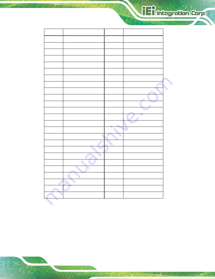
Pin
Description
Pin
Description
27
NC
28
NC
29
USB3_RX2_N
30
NC
31
USB3_RX2_P
32
NC
33
GND
34
NC
35
USB3P0_TXDNM2
36
NC
37
USB3P0_TXDPM2
38
GND
39
GND
40
NC
41
M1_S_C
42
NC
43
M1_SATA_RX1-_C
44
NC
45
GND
46
NC
47
M1_S_C
48
NC
49
M1_SATA_TX1-_C
50
NC
51
GND
52
NC
53
NC
54
GND
55
NC
56
NC
57
GND
58
NC
59
NC
60
NC
61
NC
62
NC
63
GND
64
NC
65
NC
66
NC
67
Reset
68
NC
69
NC
70
+3.3V
71
GND
72
+3.3V
73
GND
74
+3.3V
75
GND
Table 3-11: M.2 B-Key Slot Pinouts
Summary of Contents for HYPER-AL series
Page 12: ......
Page 13: ...HYPER AL SBC Page 1 Chapter 1 1 Introduction...
Page 21: ...HYPER AL SBC Page 9 Chapter 2 2 Unpacking...
Page 25: ...HYPER AL SBC Page 13 Chapter 3 3 Connectors...
Page 48: ...HYPER AL SBC Page 36 Chapter 4 4 Installation...
Page 58: ...HYPER AL SBC Page 46 Chapter 5 5 BIOS...
Page 90: ...HYPER AL SBC Page 78 Chapter 6 6 Software Drivers...
Page 94: ...HYPER AL SBC Page 82 Appendix A A Regulatory Compliance...
Page 96: ...HYPER AL SBC Page 84 B Product Disposal Appendix B...
Page 98: ...HYPER AL SBC Page 86 Appendix C C BIOS Menu Options...
Page 101: ...HYPER AL SBC Page 89 Appendix D D Digital I O Interface...
Page 104: ...HYPER AL SBC Page 92 Appendix E E Watchdog Timer...
Page 107: ...HYPER AL SBC Page 95 Appendix F F Hazardous Materials Disclosure...


