1
©2018 Integrated Device Technology, Inc.
March 7, 2018
Register Descriptions
The register descriptions section describes the behavior and function of the customer-programmable non-volatile-memory registers in the
9FGV1005 clock generator.
For details of product operation, refer to the product datasheet.
9FGV1005 Clock Register Set
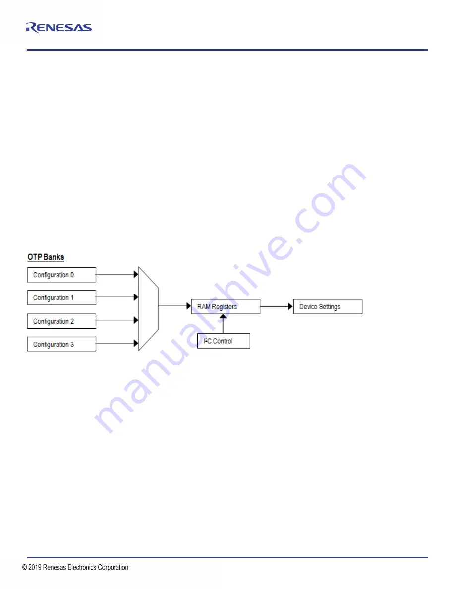
The device contains volatile (RAM) 8-bit registers and non-volatile 8-bit registers (
). The non-volatile registers are One-Time
Programmable (OTP) and will be pre-programmed at the factory with a custom dash-code configuration.
The device operates according to settings in the RAM registers. At power-up a pre-programmed configuration is transferred from OTP to
RAM registers. The device behavior can then be modified by reprogramming the RAM registers through I
2
C.
The device can start up in “I
2
C mode” or in “Hardware Select Mode”, depending upon the status of the REF0_SEL_I2C# pin at power up.
Also see the datasheet. I
2
C access is only possible when the device has started up in I
2
C mode. Startup in I
2
C mode is default when no
pull-up is added to the REF0_SEL_I2C# pin. Pre-programming settings determine which of the 4 OTP banks is loaded into RAM registers
at power up in I
2
C mode. Using I
2
C commands, the configuration can be changed and there are also commands to reload a configuration
from a different OTP bank.
Figure 1. Register Maps
User Configuration Table Selection
At power-up, the voltage at OUT0_SEL_I2CB pin 24 is latched by the part and used to select the state of SEL0/SCL and SEL1/SDA pins
(
When a weak pull-up (10k
Ω
) is placed on REF0_SEL_I2C#, the SEL0/SCL and SEL1/SDA pins will be configured as hardware select
inputs, SEL0 and SEL1. Connecting SEL0 and SEL1 to VDDD and/or GND selects one of 4 configuration register sets, CFG0 through
CFG3, which is then loaded into the non-volatile configuration registers to configure the clock synthesizer. The CFG0 through CFG3
configurations are preprogrammed at the factory according to customer specifications and assigned a specific (dash) part number.
When a weak pull-down is placed on REF0_SEL_I2C# (or when it is left floating to use internal pull-down), the pins SEL0 and SEL1 will
be configured as an I
2
C interface's SDA and SCL slave bus. Configuration register set CFG0 is commonly loaded into the non-volatile
configuration registers to configure the clock synthesizer but the device can be configured to load any of the other configurations. The
host system can use the I
2
C bus to update the volatile RAM registers to change the configuration, and to read status registers.
9FGV1005 Register Descriptions and
Programming Guide


