background image

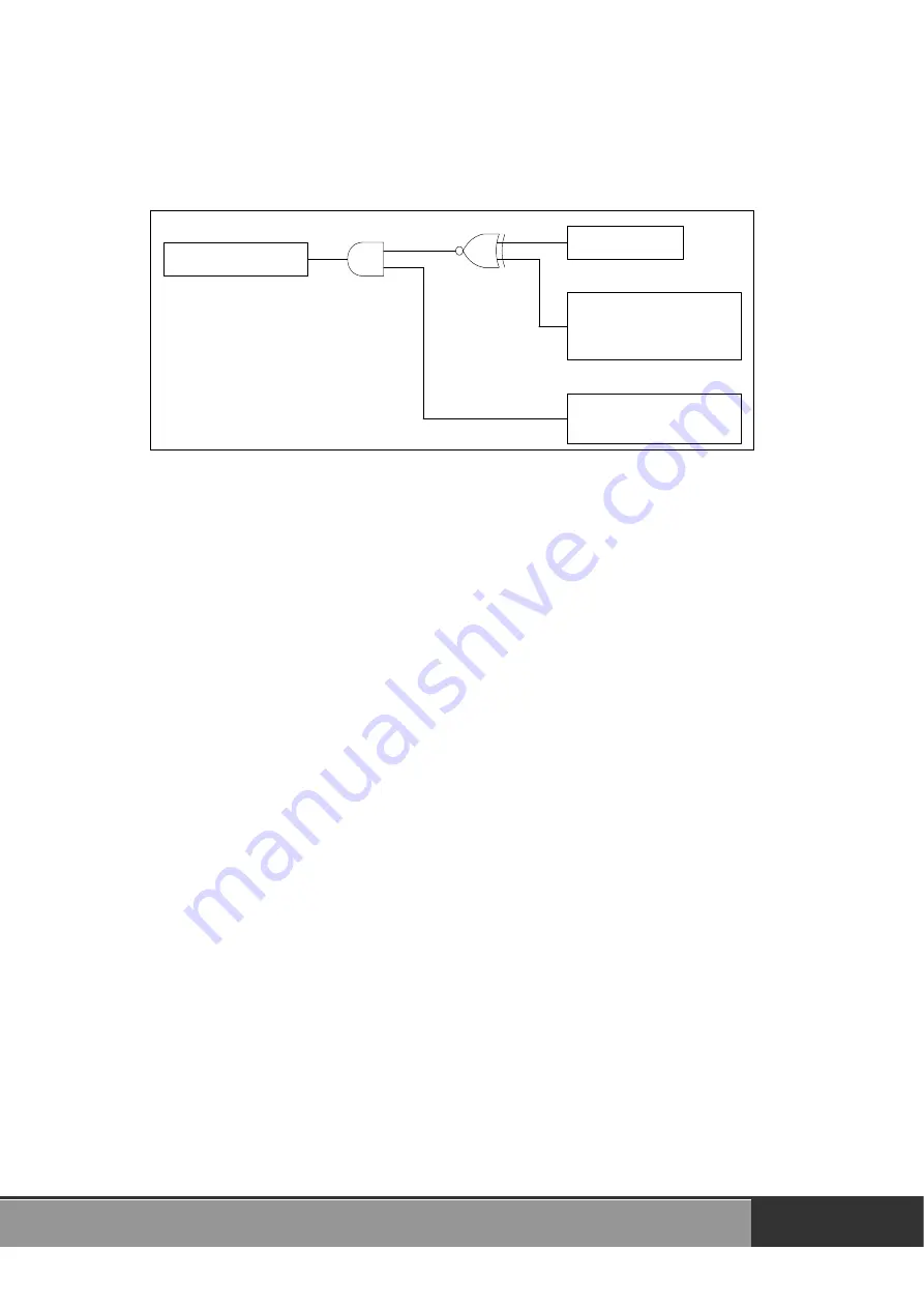
2.3.2    INT_CHAN_0/1 


INT0/1

Inverted/Noninverted

select

(INV0/1)

Enable/Disable select

(EN0/1)

INT_CHAN_0/1


 The architecture for INT_CHAN_0 and INT_CHAN_1 is shown in the above 
figure. The only difference between INT0 and INT1 is that the INT_CHAN_0 
signal source is from the 8254 counter0 output and the INT_CHAN_1 signal 
source is from the 8254 counter2 output.  
 

INT_CHAN_0/1 must be fixed at a low level state normally and a 

high_pulse generated to interrupt the PC. 

 
EN0/1 can be used to enable/disable the INT_CHAN_0/1 in the following 
manner: (Refer to Sec.3.3.4) 
EN0/1 = 0 

 INT_CHAN_0/1 = disabled 

EN0/1 = 1 

 INT_CHAN_0/1 = enabled 

 
INV0/1 can be used to invert/non-invert INT0/1 in the following manner: (Refer to 
Sec.3.3.6) 
INV0/1 = 0 

 INT_CHAN_0/1 = inverted state for INT0/1 

 INV0/1 = 1 

 INT_CHAN_0/1 = non-inverted state for INT0/1 

 
As noted above, 

if INT\ is fixed at a low level state, the PIO-DA4/8/16


will 

interrupt the PC continuously, so the interrupt service routine should use 

INV0/1 to invert/non-invert the INT0/1 in order to generate a high_pulse


(Refer to the next section) 

PIO-DA/PISO-DA Series User Manual (Ver.2.9, Feb. 2011, PMH-009-29 )    

12


Summary of Contents for PIO-DA4

Page 1: ...ICP DAS reserves the right to change this manual at any time without notice The information furnished by ICP DAS is believed to be accurate and reliable However no responsibility is assumed by ICP DA...

Page 2: ...ER BOARDS 34 3 I O CONTROL REGISTER 39 3 1 HOW TO FIND THE I O ADDRESS 39 3 2 THE ASSIGNMENT OF THE I O ADDRESSES 45 3 3 THE I O ADDRESS MAP 47 4 SOTFWARE INSTALLATION 55 4 1 SOFTWARE INSTALLING PROCE...

Page 3: ...the PISO DA series the voltage output range is from 10 V to 10 V with a current output range from 0 to 20 mA In addition the PISO DA and PIO DA series also provide the following advantages 1 Accurate...

Page 4: ...o pacer timer interrupt sources Double buffered D A latch Software calibration 16 D I channels 16 D O channels One D Sub connector two 20 pin flat cable connectors Connects directly to DB 16P DB 16R D...

Page 5: ...Logic 1 2 4 V min Output Capability Sink 2 4 mA 0 8 V Source 0 8 mA 2 0 V Response Speed 1 0 MHz Typical Timer Counter Channels 3 Resolution 16 bit Compatibility 5 V TTL Reference Clock Internal 4 MH...

Page 6: ...4C 24 channel open collector output board ADP 20 PCI extender 20 pin header to 20 pin header for PCI Bus I O 1 4 Product Checklist The shipping package includes the following items One PIO DA or PISO...

Page 7: ...DA16 Board Layout CON1 CON2 CON3 PCI BUS PIO DA16 PIO DA8 PIO DA4 1 2 19 20 1 2 19 20 DI DO CON1 16 channel D O CON2 16 channel D I CON3 4 8 16 channel D A converter voltage current output PIO DA PIS...

Page 8: ...A16U and PISO DA4U DA8U DA16U Board Layout CON1 16 channel D O CON2 16 channel D I CON3 4 8 16 channel D A converter voltage current output SW1 Card ID PIO DA PISO DA Series User Manual Ver 2 9 Feb 20...

Page 9: ...o interrupt sources The first is a 16 bit timer output INT0 and the other one is a 32 bit timer output INT1 The block diagram is shown below OUT0 CLK0 GATE0 Counter0 OUT1 CLK1 GATE1 Counter1 OUT2 CLK2...

Page 10: ...1 Read the new status of all interrupt signal sources 2 Compare the new status with the old status to identify the active signals 3 If INT0 is active service it 4 If INT1 is active service it 5 Save...

Page 11: ...nterrupt the PC The priority of INT_CHAN_0 1 is the same If both of these signals are active at the same time then INT will only be active once at a time So the interrupt service routine has to read t...

Page 12: ...C EN0 1 can be used to enable disable the INT_CHAN_0 1 in the following manner Refer to Sec 3 3 4 EN0 1 0 INT_CHAN_0 1 disabled EN0 1 1 INT_CHAN_0 1 enabled INV0 1 can be used to invert non invert INT...

Page 13: ...need to generate a high_pulse outportb wBase 0x2a 1 INV0 select the non inverted input b INT_CHAN_0 INT0 LOW INT_CHAN_0 generate a high_pulse now_int_state 0 now INT0 LOW else now_int_state 1 now INT0...

Page 14: ...OW need to generate a high_pulse outportb wBase 0x2a 1 INV0 select the non inverted input d INT_CHAN_0 INT0 LOW INT_CHAN_0 generate a high_pulse now_int_state 0 now INT0 LOW else now_int_state 1 now I...

Page 15: ...at the same time INT1 is active Refer to DEMO5 C for the source program All of these falling edge and rising edge can be detected using DEMO5 C Note When the interrupt is active the user program has t...

Page 16: ..._state compare new_state to old_state if int_c 0x01 1 INT_CHAN_0 is active if new_int_state 1 0 INT0 change to low now INT0_L else INT0 change to high now INT0_H invert invert 1 generate high_pulse if...

Page 17: ...ows Local Data Bus D I port CON2 16 bits 16 bits D O port CON1 16 bits 16 bits The D I Port can be connected to a DB 16P which is a 16 channel isolated digital input daughter board The D O Port can be...

Page 18: ...ed by the RESET signal Refer to Sec 3 3 1 for more information about the RESET signal The RESET signal is in the Low state all DI operations are disabled The RESET signal is in the High state all DI o...

Page 19: ...o clear the DO states Refer to Sec 3 3 1 for more information about the RESET signal The RESET signal is in the Low state all DO channels are cleared to the low state The block diagram of DO is as fol...

Page 20: ...13 Current Output 14 Current Output 15 Voltage Output 15 Voltage Output 14 Voltage Output 13 Voltage Output 12 Voltage Output 11 Voltage Output 10 Voltage Output 9 Voltage Output 7 Voltage Output 6 Vo...

Page 21: ...some calibration when changing from voltage to current Also if these VRs are changed the user has to re perform the calibration This procedure is complex and creates a heavy workload The PISO DA PIO D...

Page 22: ...to send Vout volts to Channel n the calibrated hex value DaValue sent to D A converter can be calculated in the following way DeltaV n 20 0 MaxV n MinV n DeltaV n volts per count at channel_n DaValue...

Page 23: ...0X1FFF 0X25D0 10 1V 10 1V 22mA 0V 5 05V 5 05V 5 05V 0V 22mA 0mA 4mA 10 1V Voltage Channel Output Current Channel Output The resolution for each range is as follows Configuration Equivalent Bits Resolu...

Page 24: ...ff to 0x2fff which means that the resolution is about 13 bits 2 6 4 0 10 V Voltage Output The voltage output for PISO DA PIO DA series cards is always in the range of 10 V 1 If the user needs to outpu...

Page 25: ...t described in Sec 2 6 Iout will be in the range of 4 20 mA so the DaValue will approximately be from 0x2600 to 0x3fff which means that the resolution is about 13 bits 2 6 8 No VR No Jumper Design In...

Page 26: ...uivalent Bits Resolution 10 V 10 V 14 bit 1 22 mV 0 V 10 V 13 bit 1 22 mV 5 V 5 V 13 bit 1 22 mV 0 V 5 V 12 bit 1 22 mV 0 mA 20 mA 13 bit 2 70 A 4 mA 20 mA 13 bit 2 70 A All these VRs and jumpers have...

Page 27: ...for channel_n are as follows Step 1 DaValue 0 Step 2 Send the DaValue to channel_n on the PIO PISO card Step 3 Measure the voltage of channel_n on the I 7017 If this value is 10 V then go to Step 5 St...

Page 28: ...tep 5 Step 4 Increase the DaValue the return to Step 2 Step 5 MinI n DaValue 1 Step 6 DaValue 0x3fff Step 7 Send the DaValue to channel_n on the PIO PISO card Step 8 Measure the current of channel_n o...

Page 29: ...Step 5 Repeat Step 4 for each channel After this procedure the new data for MinV n MaxV n MinI n MaxI n will be stored in the onboard EEPROM DEMO10 EXE can be executed to back up the old calibration d...

Page 30: ...Data D A Converter D0 D13 Vout Amp AGND Output Current Max 5mA Load Internal External 2 6 11 Voltage Output Connection 2 6 12 Current Output Connection Load 14 bits Data D A Converter D0 D13 Vout Amp...

Page 31: ...B 5 V 20 PCB 12 V CON2 Digital input connector Pin Name Pin Name 1 Digital Input 0 2 Digital Input 1 3 Digital Input 2 4 Digital Input 3 5 Digital Input 4 6 Digital Input 5 7 Digital Input 6 8 Digital...

Page 32: ...round 6 Voltage Output 4 25 Current Output 4 7 Voltage Output 5 26 Current Output 5 8 Voltage Output 6 27 Current Output 6 9 Voltage Output 7 28 Current Output 7 10 Analog ground 29 Analog ground 11 V...

Page 33: ...ut 7 10 Analog ground 29 N A 11 Voltage Output 8 30 Current Output 8 12 Voltage Output 9 31 Current Output 9 13 Voltage Output 10 32 Current Output 10 14 Voltage Output 11 33 Current Output 11 15 Anal...

Page 34: ...37 The DN 37 is a general purpose daughter board for the DB 37 using DIN Rail Mounting and is designed for easy wiring 2 8 3 DB 8125 The DB 8125 is a general purpose screw terminal board and is design...

Page 35: ...an be used to sense DC signals from TTL levels up to 24 V or to sense a wide range of AC signals This board can also be used to isolate the host computer from large common mode voltages ground loops a...

Page 36: ...al to the appropriate relay channel via the 20 pin flat cable connector There are 16 LEDs one for each relay which are illuminated when their associated relay is activated To avoid overloading the pow...

Page 37: ...relays or 50 pin flat cable connector OPTO 22 compatible for the DIO 24 series There are 24 LEDs one for each relay which are illuminated when their associated relay is activated To avoid overloading...

Page 38: ...o Yes No DB 24PD No Yes Yes DB 16P8R No Yes Yes DB 24R No Yes No DB 24RD No Yes Yes DB 24C Yes Yes Yes DB 24PR Yes Yes No Db 24PRD No Yes Yes DB 24POR Yes Yes Yes DB 24SSR No Yes Yes Note There is no...

Page 39: ...U Version Rev1 0 Rev3 0 Rev4 0 above Rev1 0 above Rev1 0 above Vendor ID 0xE159 0xE159 0xE159 0xE159 Device ID 0x02 0x01 0x01 0x01 Sub Vendor ID 0x80 0x4180 0x4180 0x4180 Sub Device ID 0x04 0x00 0x00...

Page 40: ...information wSubVendor The subVendor ID of this board wSubDevice The subDevice ID of this board wSubAux The subAux ID of this board 3 Physical slot information wSlotBus The bus number of the slot use...

Page 41: ...ry Sample program 1 Detect all PIO DA4 8 16 series cards installed in this PC Step 1 Detect all PIO DA16 8 4 series cards installed in this PC wSubVendor 0x80 wSubDevice 4 wSubAux 0x00 For PIO DA4 8 1...

Page 42: ...rds in this PC wBoards if wBoards 0 exit 0 Step 2 Save the resource information for all PIO PISO cards installed in this PC printf n for i 0 i wBoards i PIO_GetConfigAddressSpace i wBase wIrq wSubVend...

Page 43: ...d in this system The application program can then directly control all functions of the PIO PISO series card Detect the configuration address space for your PIO DA4 8 16 series cards Step 1 Detect all...

Page 44: ...s function will display a text string showing these special subIDs which are the same as those defined in the PIO H include file The code for the demo program is as follows Detect all PIO_PISO series...

Page 45: ...ard_0 is to use the wSlotBus and wSlotDevice functions in the following manner Step 1 Remove all PIO DA4 8 16 series cards from the PC Step 2 Install a PIO DA4 8 16 series card into PCI_slot1 on the P...

Page 46: ...rmation for all slots in the PC This mapping is fixed for each PC and can then be used to identify a specific PIO PISO card in the following manner Step 1 Record all wSlotBus and wSlotDevice informati...

Page 47: ...wBase 0xcc Read 8254 control word Write 8254 control word wBase 0xd4 Read the Card ID Reserved wBase 0xe0 Read the low byte of the D I DA_0 chip select wBase 0xe4 Read the high byte of the D I DA_1 ch...

Page 48: ...7 Bit 6 Bit 5 Bit 4 Bit 3 Bit 2 Bit 1 Bit 0 Aux7 Aux6 Aux5 Aux4 Aux3 Aux2 Aux1 Aux0 Note Refer to Sec 3 1 for more information regarding wBase When the PC is first power on all Aux signals are in the...

Page 49: ...b wBase 5 2 Enable the interrupt of INT1 outportb wBase 5 3 Enable both interrupt channels Refer to the following demo programs for more information DEMO3 C and DEMO4 C single interrupt source DEMO5 C...

Page 50: ...Interrupt Polarity Control Register Write wBase 0x2A Bit 7 Bit 6 Bit 5 Bit 4 Bit 3 Bit 2 Bit 1 Bit 0 0 0 0 0 INV1 INV0 Note Refer to Sec 3 1 for more information regarding wBase INV0 1 0 select the i...

Page 51: ...iValue wDiHiByte 8 wDiLoByte Refer to the DEMO2 C file for more information 3 3 9 Digital Output Write wBase 0xf8 Low byte of the D O port Bit7 Bit6 Bit5 Bit4 Bit3 Bit2 Bit1 Bit0 DO7 DO6 DO5 DO4 DO3 D...

Page 52: ...rate generator 011 mode3 square wave generator 100 mode4 software triggered pulse 101 mode5 hardware triggered pulse SC1 SC0 00 counter0 01 counter1 10 counter2 11 read back command WORD pio_da16_c0 c...

Page 53: ...base 0xe4 DA_1 1 1 D A output channel 7 0 0 D A output channel 8 0 1 D A output channel 9 1 0 D A output channel10 Wbase 0xe8 DA_2 1 1 D A output channel11 0 0 D A output channel12 0 1 D A output chan...

Page 54: ...Select the D A converter Start the conversion outportb wBase 0xf0 wDaValue output low byte of D A data outportb wBase 0xf4 wDaValue 8 0x02 output high byte of D A data and select channel 2 on this con...

Page 55: ...the AUTO32 EXE file in the NAPDOS folder on this CD Step 2 Click the item PCI Bus DAQ Card Step 3 Click the item UniDAQ Step 4 Click the item DLL for Windows 2000 and XP 2003 Vista 32 bit Step 5 Doub...

Page 56: ...ile will be copied into the C WINNT SYSTEM32 folder The NAPWNT SYS and PIODA SYS files will be copied into the C WINNT SYSTEM32 DRIVERS folder Windows 95 98 ME The PIODA DLL and PIODA Vxd files will b...

Page 57: ...ws Step 1 Select Start Control Panel and then double click the System icon on Windows Step 2 Click the Hardware tab and then click the Device Manager button Step 3 Check the PIO DA or PISO DA series c...

Page 58: ...L driver installation process the install shield will register the correct kernel driver to the operating system and copy the DLL driver and demo programs to the correct location depending on the driv...

Page 59: ...ation file TC LIB Large TCPIO_L LIB TC large model library file TC LIB Huge PIO H TC declaration file TC LIB Huge TCPIO_H LIB TC huge model library file MSC for MSC 5 xx or above MSC LIB Large PIO H M...

Page 60: ...rator without calibration DEMO7 EXE Waveform generator with calibration DEMO8 EXE D A hex value output without calibration DEMO9 EXE D A hex value output with calibration DEMO10 EXE Save EEPROM data t...

Page 61: ...cards that are installed in the PC will be shown as illustrated below Note The PIO_PISO EXE application is valid for all PIO PISO cards The user can execute the PIO_PISO EXE file to retrieve the follo...

Page 62: ...0 i wBoards i PIO_GetConfigAddressSpace i wBase wIrq wSubVendor wSubDevice wSubAux wSlotBus wSlotDevice printf nCard_ d wBase x wIrq x subID x x x SlotID x x i wBase wIrq wSubVendor wSubDevice wSubAu...

Page 63: ...O cards Step 2 enable all D I O port outportb wBase 1 RESET 1 printf n n 2 DEMO2 D I O test j 1 for pio_da16_do j pio_da16_di k gotoxy 1 9 printf DO 4x DI 4x j k if k j printf Test Error else printf T...

Page 64: ...ng of PIO PISO cards Step 2 enable all D I O port outportb wBase 1 RESET 1 printf n n 2 DEMO3 Interrupt 1Hz test init_int1_high interrupt initialize INT1 is high now COUNT_L 0 COUNT_H 0 printf n n Sho...

Page 65: ...low need to generate a high pulse outportb wBase 0x2a 2 INV1 select non inverted input INT_CHAN_1 INT1 low INT_CHAN_1 generate high pulse now_int_state 0 now INT1 low else now_int_state 1 now INT1 hig...

Page 66: ...n n 2 DEMO5 Interrupt test init_high interrupt initialize INT_CHAN_0 1 is high now printf n n Show the count of Low_pulse n INT0_L INT0_H INT1_L INT1_H 0 for gotoxy 1 10 printf nINT0 x x INT1 x x INT...

Page 67: ...the interrupt status again to identify the active interrupt source 3 The INT_CHAN_0 INT_CHAN_1 can be active at the same time void interrupt irq_service now ISR can not know which interrupt is active...

Page 68: ...test printf n n a 1 23V Voltage output to each channel for i 0 i 16 i j 1 23 16383 20 0 8192 pio_da16_da i j getch printf n n b 1 23mA Current output to each channel for i 0 i 16 i j 1 23 8192 20 819...

Page 69: ...nd address mapping of PIO PISO cards Step 2 enable all D I O port outportb wBase 0x11 RESET 1 outportb wBase 2 0x1c AUX 4 3 2 are D O othes D I outportb wBase 3 0 all D O are Low printf n n 2 A D Outp...

Page 70: ...getch printf n n b 1 23mA Current output to each channel for i 0 i 16 i j 1 23 fDeltaI i w00mA i pio_da16_da i j getch outportb wBase 5 0 disable all interrupt outportb wBase 3 0 all D O are Low outp...

Reviews: