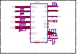
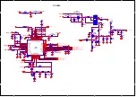
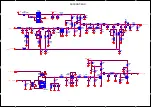
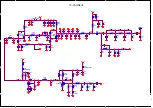
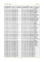
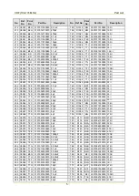
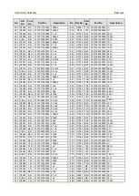
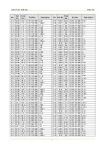
Hytera PD502 Service Manual Download Page 66

VHF (136-174 MHz) 

Part List 


No.    Ref 

No.   

Print 

No. 

Part No. 

Description    No.    Ref No.   Print 

No. 

Part No. 

Description 

266  C6102  T3C  3101055600000  56pF 

  779  R314  T2A  3001050000000  0

Ω


267  C6103  T2D  3101055600000  56pF 

  780  R316  B2G  3001050000000  0

Ω


268  C6104  T2D  3101055600000  56pF 

  781  R317  T2B  3001050000000  0

Ω


269  C7002  B4E  3101052230000  0.022uF 

  782  R318  B2E  3001054740010  470K

Ω


270  C7003  B4F  3101061020000  1000pF 

  783  R319  B2E  3001054730010  47K

Ω


271  C7004  B4F  3101054710010  470pF 

  784  R320  B1F  3001051040000  100K 

272  C7005  B3F  3101054710010  470pF 

  785  R321  B1F  3001051040000  100K 

273  C7006  B4F  3101052220010  2200pF 

  786  R322  B4G  3001051030050  10K

Ω


274  C7007  T3E  3101051040060  0.1uF 

  787  R323  T2B  3001051040000  100K 

275  C7008  T3E  3101051020010  1000pF 

  788  R324  B2K  3001054720000  4.7K

Ω


276  C7009  T3D  3101054700010  47pF 

  789  R326  B2H  3001050000000  0

Ω


277  C7010  T3D  3101051020010  1000pF 

  790  R327  B2I  3001058220010  8.2K

Ω


278  C7011  T3D  3101051040060  0.1uF 

  791  R328  B2H  3001050000000  0

Ω


279  C7012  T3D  3101081060010  10uF 

  792  R330  B4G  3001051040000  100K 

280  C7013  T4C  3101051020010  1000pF 

  793  R331  B3F  3001051040000  100K 

281  C7014  T4C  3101051040060  0.1uF 

  794  R332  B2F  3001051010040  100

Ω


282  C7015  B4E  3101051010030  100pF 

  795  R333  B2K  3001050000000  0

Ω


283  C7016  B4E  3101061020000  1000pF 

  796  R6001  T3H  3001011030080  10K

Ω


284  C7018  T4E  3101051020010  1000pF 

  797  R6002  T2H  3001011020060  1K

Ω


285  C7019  B4F  3101054710010  470pF 

  798  R6003  T2H  3001018230000  82K

Ω


286  C7020  T4C  3101062700010  27pF 

  799  R6004  T3H  3001051510000  150

Ω


287  C7022  T4C  3101060700020  7pF 

  800  R6005  T3H  3001051220090  1.2K 

288  C7024  T3B  3101060600010  6pF 

  801  R6006  T2H  3001017520020  7.5K

Ω


289  C7025  T3C  3101060900010  9pF 

  802  R6007  T2H  3001011010080  100

Ω


290  C7026  T2B  3101062790000  2.7pF 

  803  R6008  T2I  3001014720050  4.7K

Ω


291  C7028  T4C  3101062210000  220pF 

  804  R6009  B3G  3001015100060  51

Ω


292  C7029  T3C  3101061020000  1000pF 

  805  R6010  T3H  3001011030080  10K

Ω


293  C7031  T4E  3101061010010  100pF 

  806  R6011  T3G  3001013910000  39

Ω


294  C7036  T4B  3101061000000  10pF 

  807  R6012  B2H  3001011030080  10K

Ω


295  C7037  T3C  3101060800010  8pF 

  808  R6013  B3I  3001011040030  100K

Ω


296  C7038  T3C  3101051020010  1000pF 

  809  R6014  B3I  3001011820000  1.8K

Ω


297  C7039  T3B  3101062400010  24pF 

  810  R6015  B3H  3001052720010  2.7K

Ω


298  C7041  T3B  3101062000000  20pF 

  811  R6016  B3I  3001061030010  10K

Ω


299  C7042  T2B  3101061020000  1000pF 

  812  R6017  B3H  3001058210000  820

Ω


300  C7043  T2B  3101061100010  11pF 

  813  R6018  T2G  3001051010040  100

Ω


301  C7044  T4C  3101060500010  5pF 

  814  R6019  T3G  3001058230000  82K

Ω


302  C7048  T5E  3101062400010  24pF 

  815  R6020  T3D  3001011030080  10K

Ω


303  C7050  T5E  3101051040060  0.1uF 

  816  R6022  T2D  3001016810020  680

Ω


304  C7051  T5E  3101054710010  470pF 

  817  R6023  T2D  3001015620030  5.6K

Ω


305  C7052  T3C  3101051000020  10pF 

  818  R6024  T2D  3001011040030  100K

Ω


306  C7057  T4G  3101051020010  1000pF 

  819  R6025  T2D  3001011040030  100K

Ω


307  C7058  T4G  3101051040060  0.1uF 

  820  R6026  T3C  3001011040030  100K

Ω


308  C7059  T4F  3101052200010  22pF 

  821  R6027  T2C  3001011040030  100K

Ω


309  C7060  T4F  3101051500020  15pF 

  822  R6028  T3C  3001011040030  100K

Ω


310  C7061  T4G  3101051020010  1000pF 

  823  R6029  T2D  3001011030080  10K

Ω


311  C7062  T4G  3101051020010  1000pF 

  824  R6030  T1G  3001055610000  560

Ω


312  C7063  T4G  3101052700000  27pF 

  825  R6031  T1G  3001013920030  3.9K

Ω


313  C7065  T4D  3101065600040  56pF 

  826  R6033  T2G  3001053310000  330

Ω


314  C7066  T4C  3101061100010  11pF 

  827  R6034  T1H  3001013330010  33K

Ω


315  C7068  T4F  3101051020010  1000pF 

  828  R6035  T2G  3001015100060  51

Ω


316  C7069  T4F  3101051020010  1000pF 

  829  R6038  T2G  3001011030080  10K

Ω


317  C7071  T4E  3101061800000  18pF 

  830  R6040  T1E  3001015100060  51

Ω


318  C8001  B4I  3101011040080  0.1uF 

  831  R6042  T1H  3001011040030  100K

Ω


319  C8003  B4I  3101011040080  0.1uF 

  832  R6043  T2G  3001015630000  56K

Ω


Summary of Contents for PD502

Page 1: ...PORTABLE...

Page 2: ...e product repair It is intended for use by qualified technicians only To repair the product properly please read this manual carefully before repairing This manual is applicable to the following produ...

Page 3: ...y rights including patent rights copyrights and trade secrets of Digital Voice Systems Inc This voice coding technology is licensed solely for use within this product The user of this technology is ex...

Page 4: ...s situations that could cause major personal injury or even death Notational Conventions Convention Description The quotation marks enclose the name of a software interface element For example click O...

Page 5: ...VHF 136 174 MHz...

Page 6: ...dule 18 5 2 RF Section 19 5 2 1 Transmitter Circuit 19 5 2 2 Receiver Circuit 20 5 2 3 FGU 22 6 Troubleshooting Flow Chart 24 6 1 Control Circuit 24 6 2 Receiver Circuit 26 6 3 Transmitter Circuit 27...

Page 7: ...Controls No Part Name No Part Name 1 PTT Push to Talk Key 7 Accessory connector 2 SK1 Side Key 1 8 Microphone 3 Channel Selector Knob 9 Battery Latch 4 Speaker 10 Antenna 5 LED Indicator 11 Belt Clip...

Page 8: ...roof ring properly during reassembly After reassembly please check the waterproof performance of the radio using the waterproof test instrument specified by the Company Step 1 Remove the battery Step...

Page 9: ...4 MHz Disassembly and Assembly 3 Step 4 Loosen the two screws on the bottom of the aluminum chassis Step 5 Remove the aluminum chassis along with the main board Step 6 Loosen the seven screws on the m...

Page 10: ...VHF 136 174 MHz Disassembly and Assembly 4 Step 7 Desolder the soldering joint of the antenna and remove the main board...

Page 11: ...8 6201905000000 Speaker fixing sheet 1 28 7500272000000 Heat sink pad 1 9 7400633000000 Speaker supporting PC sheet 1 29 6100505000010 Waterproof ring for battery connector 1 10 4323020000020 Volume s...

Page 12: ...VHF 136 174 MHz Exploded View and Packaging Guide 6 Note Parts that are not marked with Part Number may vary with the frequency band...

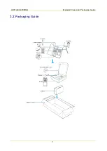
Page 13: ...VHF 136 174 MHz Exploded View and Packaging Guide 7 3 2 Packaging Guide...

Page 14: ...rs Digital 15 hours Operating Temperature 30 to 60 Dimension H W D with standard battey without antenna 117 55 28 mm Weight with antenna standard battey About 280 g Frequency Stability 1 5 ppm Receive...

Page 15: ...due to continuous development Blocking 84 dB Rated Audio Power Output 0 5 W 16 load Rated Audio Distortion 3 Transmitter Power Output 5 W 1 W Conducted Radiated Emission 36 dBm 1 GHz 30 dBm 1 GHz Mod...

Page 16: ...0M 1 1V 2 5 V Externa l 2 3V 2 5V 2 7V Pro 2 5 V 1 25V Pro 1 25V 0 5V 6 V 3V 3 3V 3 6V 3V 4 2V 3V 3 3V 3 6V VDDQ1 7V 1 8V 1 95 V Operation Mode SDRAM VDDQ2 7V 3 1 V Read while write Nor Flash PsRAM VC...

Page 17: ...nd the power is cut off Power Protection Power protection includes over current reverse voltage and ESD protection Power Consumption Control OMAP can control and configure the power supply and working...

Page 18: ...VHF 136 174 MHz Circuit Description 12...

Page 19: ...PWM0 PWT uWire BCLK 19 2MHz McBSP3 McBSP2 TX MCSI1 GPIO CS0 CS3 UART1 To PLL TX DAC TLV5614 CS1 McBSP1 CS0 MCLK BUZZ_IN USB IF APC Final_bias MOD TX_RF_CS 32 768KHz XTAL UART3 UART2 I2C IF RX AD9864...

Page 20: ...5 A0 A10 SDRAM BA1 SDRAM BA0 CAS SDRAM CS RAS LDQM UDQM WE CLK CKE A1 A24 D0 D15 RESET OE WE WP FLASH RDY CE EMIFS EMIFS can support 16 bit external device width and provides four chip selects CS0 CS3...

Page 21: ...system timing and sleeping 19 2 MHz Clock It is the system clock and is mainly used for providing input clock for APLL and DPLL Output Clock There is one output clock MCLK MCLK provides 16 MHz clock t...

Page 22: ...works in master mode MCBSP3 is connected to the interface for option board The connection of MCBSP is shown below MCBSP3 FSX P18 MCBSP3 DX W14 MCBSP3 DR AA17 MCBSP2 CLKX Y6 MCBSP2 FSX W7 CODEC IIS_WCL...

Page 23: ...C is shown below MICROWIRE OMAP5912 provides a MICROWIRE The four chip selects can drive four external components MICROWIRE is used to configure the audio codec and read the value of its register It...

Page 24: ...decoding digital signal decoding and digital audio signal processing AD9864 converts and processes the RF IF signal and sends the undemodulated serial digital signal to the DSP for processing Then TLV...

Page 25: ...y DAC of the codec Finally the signal is amplified by the external audio amplifier TDA2822 to drive the speaker and the audio signal is output OMAP5912 Audio is processed via DSP UWIRE SCLK UWIRE CS3...

Page 26: ...multiple amplifiers the signal will pass through a microstrip matcher to complete output impedance matching so as to reduce output power loss due to impedance mismatch Step 4 Finally the signal passes...

Page 27: ...of band interference signal and to send wanted band pass signal to the low noise amplifier Q6005 The amplified signal goes to a band pass filter controlled via APC TV1 level to remove out of band inte...

Page 28: ...AP5912 for demodulation AD9864 employs reference frequency of 19 2 MHz and shares the crystal with OMAP The second LO VCO comprises an oscillator a varactor and some other components to provide the LO...

Page 29: ...voltage is sent to the varactor of VCO It adjusts the output frequency of VCO directly until the CV voltage becomes constant Then PLL is locked and the stable frequency output by VCO goes to the TX R...

Page 30: ...U306 U303 and control circuit LED works normally 3V3D is normal Replace LED Check U2013 U309 Reset Check U305 Yes No Yes No Yes Yes No No Yes No No 19 2MHz crystal oscillator is normal 3 The control c...

Page 31: ...shooting Flow Chart 25 1 After the radio powers on the LED indicator and alert tone works properly 2 The RF power supply outputs normally and the RX channel is on 3 Output by the crystal oscillator Vp...

Page 32: ...05 Check Q6006 Q6007 The static working point of Q6005 is normal 3 The static working point of Q6006 Q6007 is normal 4 Input IF signal via U6001PIN47 to check whether IF sensitivity is normal 5 18MHz...

Page 33: ...he IF sensitivity is 109 dBm 6 Frequency of Q6003 44 85 MHz 7 Frequency of L6013 18 MHz 8 Input a 30 dBm RF signal and test at RP1 Normally gain 10 dB output signal 20 dBm 9 Input a 30 dBm RF signal i...

Page 34: ...ower is normal Power is normal Power is normal Repair damaged components Power is normal TV APC is normal 3 Check the power supply circuit TX_En is normal 5 TX_En 3 3V is normal 4 Replace Q7001 and U7...

Page 35: ...The low pass coil must be soldered appropriately and remain in good condition The spring plate for the antenna must well fit the antenna connector 8 The match components must not be soldered inappropt...

Page 36: ...al oscillates Check 19 2MHz circuit Sky 72310 clock is normal 6 CV is normal 3 Replace Q8007 Q8007 is normal 5 L8018 L8045 is normal 4 Replace L8018 L8045 Replace Q8004 Q8008 Q8004 Q8008 is normal 2 Q...

Page 37: ...2 During transmission voltage at Q8008 E about 1 8 V During reception voltage at Q8004 E about 1 8 V 3 The CV value varies with frequencies Generally it is within the range 0 5 4 5 V 4 L8018 L8045 is...

Page 38: ...erface Definition 32 7 Interface Definition 7 1 J801 and J802 Double Pin Interface for Earpiece Programming and Downloading Pin Pin No Signal Function J801 1 SPK 2 USB 3 SPK 4 SPK 5 SPK J802 1 GND 2 M...

Page 39: ...TA TX and double click Reference Oscillator Warp from the navigation tree on the left Then click the Transmit On button 3 Observe the frequency displayed on HP8921 and adjust the vernier on Tuner unti...

Page 40: ...deviation is 5 k 50 Hz 5 Click the Transmit Off button 6 Click the Save button to save your settings Modulation Balance 1 Connect the antenna connector of the radio with HP8921 and set HP8921 to TX t...

Page 41: ...z De Emphasis 750 us 4 Observe the value displayed on the HP8921 and adjust the vernier on the Tuner until the SINAD value is more than 14 dB 5 Set the HP8921 parameters as follows Output RF signal 25...

Page 42: ...Hz Transmit Power 4 7 0 3 W FSK Error 5 Magnitude Error 1 Receiving Step 1 Open the Tuner software and go to TEST RX and double click Receiver BER 0 153 from the navigation tree on the left to open Re...

Page 43: ...PCB 3 9 PCB VHF 136 174 MHz...

Page 44: ...PCB 3 VHF 136 174 MHz...

Page 45: ...VHF 136 174 MHz Block Diagram 3 10 Block Diagram Radio General Diagram OMAP RX FGU Power Supply CODE TLV320AIC29IRGZ IF Processor ADC9864 SDRAM Flash TX MIC SPK Baseband Switch...

Page 46: ...d attenuation 54dBc AD9864 Band pass Filter1 Low Noise Amp Band pass Filter2 Mixer IF Filter IF Processor IF Amp OSC level 4dBm S21 12dB NF 3dB Stop band attenuation 2 IF1st 80dBc IIP3 5dBm TV1 APC S2...

Page 47: ...TV APC OMAP MCBSP2 BB System Audio Codec TLV320AIC29IRGZ OMAP5912 E M I F S E M I F F Nor FLASH and PsRAM 128MBit 32MBit S29GL128S10GHIV20 Mobile SDRAM 128Mb 8Mx16 W987D6HBGX6I Datax16 Datax16 Speed 9...

Page 48: ...65V 1 8V 1 95V 2V 3 6V MCLK 100M 2V 3 6V MCLK 50M 1 1V 2 5V External 2 3V 2 5V 2 7V Pro 2 5V 1 25V Pro 1 25V 0 5V 6V 3V 3 3V 3 6V 3V 4 2V 3V 3 3V 3 6V VDDQ 1 7V 1 8V 1 95V Operation Mode SDRAM VDDQ 2...

Page 49: ...2 OSC32K_OUT AA13 OSC32K_IN V13 CLK32K_IN P13 OSC1_OUT W3 OSC1_IN Y2 MPU_RST U20 PWRON_RESET R12 MCLK GPIO24 V5 BCLK GPIO17 Y15 CLK32K_OUT GPIO36 MPUIO0 UART1 TX R13 BFAIL EXT_FIQ UART3 CTS W19 RST_OU...

Page 50: ...MPUIO6 W11 GPIO58 R11 GPIO6 MCSI1 DIN TIMER EVENT3 P19 GPIO4 SPIF DIN TIMER EVENT4 P20 GPIO29 LCD P8 D17 GPIO30 LCD P9 D16 GPIO31 LCD P10 C17 GPIO32 LCD P11 B17 GPIO33 LCD P12 G13 GPIO34 LCD P13 A17...

Page 51: ...1 270pF C1049 0 1uF C1049 0 1uF C1055 0 22uF C1055 0 22uF R1025 NC R1025 NC C1050 0 1uF C1050 0 1uF U1002A OMAP5912ZZG 1 U1002A OMAP5912ZZG 1 FLASH A1 J8 FLASH A2 D3 FLASH A3 C1 FLASH A4 E4 FLASH A5 D...

Page 52: ...O19 AA5 MCBSP2 DX GPIO22 P10 KP R0 MPUIO8 G18 KP R1 MPUIO9 F19 KP R2 MPUIO10 H14 KP R3 MPUIO13 E20 KP R4 MPUIO15 E19 KB C0 MPUIO0 F18 KB C1 MPUIO6 D20 KB C2 GPIO61 D19 KB C3 GPIO63 E18 KB C4 GPIO27 C2...

Page 53: ...2 CE 3 Nc 1 Vout 5 C316 4 7u C316 4 7u F300 3A 32V F300 3A 32V 1 2 R308 47k R308 47k C348 22uF C348 22uF TP303 TP303 1 TP307 TP307 1 C339 2 2u C339 2 2u C355 0 1u C355 0 1u C307 0 22u C307 0 22u C327...

Page 54: ...R803 10k TP812 TP812 1 C830 0 1u C830 0 1u L808 BLM18AG601SN1 L808 BLM18AG601SN1 C802 0 01u C802 0 01u D803 PESD12VS1UB D803 PESD12VS1UB TP805 SPK TP805 SPK 1 D806 1SS356 D806 1SS356 1 2 C807 0 1u C80...

Page 55: ...K R6003 82K C6011 0 022uF C6011 0 022uF D6002 HVC350B D6002 HVC350B 2 1 C6013 0 01uF C6013 0 01uF L6011 4 7uH L6011 4 7uH C6047 39pF C6047 39pF L6001 BLM18AG601SN1 L6001 BLM18AG601SN1 C6037 0 01uF C60...

Page 56: ...C6101 120pF C6071 NC C6071 NC C6074 2 7pF C6074 2 7pF C6093 270pF C6093 270pF R6035 51 R6035 51 R6047 5 6 R6047 5 6 C6070 NC C6070 NC L6022 17nH L6022 17nH L6030 82nH L6030 82nH L6028 470nH L6028 470...

Page 57: ...NC C7016 1000pF C7016 1000pF C7004 470pF C7004 470pF R7005 1k R7005 1k C7019 470pF C7019 470pF R7049 1K R7049 1K R7050 0 R7050 0 Q7010 EM6M2 Q7010 EM6M2 6 2 1 4 5 3 R7041 150K R7041 150K DTC114EE Q70...

Page 58: ...3k C7043 1 5p C7043 1 5p C7032 NC C7032 NC L7012 BLM18AG601SN1 L7012 BLM18AG601SN1 Q7003 RD07MUS2B Q7003 RD07MUS2B 3 1 2 C7061 470pF C7061 470pF L7007 NC BLM15PD121SN1 L7007 NC BLM15PD121SN1 1 2 L7906...

Page 59: ...53 1uF C8053 1uF VCC OUT VCONT GND X8001 DSA321SDA VCC OUT VCONT GND X8001 DSA321SDA 1 2 3 4 5 6 C8013 0 1uF C8013 0 1uF C8033 1uF C8033 1uF R8020 1k R8020 1k C8028 470pF C8028 470pF U8004 TLV5614IPW...

Page 60: ...8047 82K R8047 82K C8143 6pF C8143 6pF R8051 8 2k R8051 8 2k C8073 470pF C8073 470pF C8100 120pF C8100 120pF R8063 5 6 R8063 5 6 C8112 NC C8112 NC C8111 NC C8111 NC C8096 33pF C8096 33pF D8014 HVC131...

Page 61: ...3101051040060 0 1uF 534 D8017 T3H 3399030000010 PIN diode 22 C1022 T1J 3101012240010 0 22uF 535 D8019 T5H 3304010100180 Varactor 23 C1023 T1J 3101051050160 1uF 536 D802 B2C 3399040600020 ESD protecti...

Page 62: ...L6012 B2H 3221505121010 Ferrite bead 73 C1069 B3J 3101052710000 270pF 586 L6013 B3H 3217107392000 3 9uH 74 C1070 T2K 3101052710000 270pF 587 L6014 T3G 3221505121010 Ferrite bead 75 C1071 B3J 310105271...

Page 63: ...0000 4 7uF 645 L8024 B2G 3221505121010 Ferrite bead 133 C343 B4F 3101051010030 100pF 646 L8025 T4H 3217106781000 780nH 134 C344 B4F 3101061050020 1uF 647 L8026 B4F 3210306101000 100nH 135 C345 B4F 310...

Page 64: ...8 Q8004 T4I 3408002000080 NPN transistor 186 C6011 T2H 3101012230010 0 022uF 699 Q8005 B2G 3403999000070 Compound transistor 187 C6012 T3H 3101054700010 47pF 700 Q8006 B3G 3609003999000 MMIC amplifier...

Page 65: ...9 R1045 T3K 3001013300000 33 237 C6063 T2C 3101052000020 20pF 750 R1046 B1D 3001053300000 33 238 C6064 T2C 3101050600010 6pF 751 R1047 B2J 3001011030080 10K 239 C6065 T2C 3101052000020 20pF 752 R1048...

Page 66: ...0050 4 7K 291 C7028 T4C 3101062210000 220pF 804 R6009 B3G 3001015100060 51 292 C7029 T3C 3101061020000 1000pF 805 R6010 T3H 3001011030080 10K 293 C7031 T4E 3101061010010 100pF 806 R6011 T3G 3001013910...

Page 67: ...7 R7030 T4F 3001055100020 51 345 C803 B2J 3101052240010 0 22uF 858 R7031 T4G 3001055620000 5 6K 346 C8030 B4H 3101073940000 0 39uF 859 R7032 B4F 3001051210010 120 347 C8031 B4H 3101073940000 0 39uF 86...

Page 68: ...101053900000 39pF 911 R8033 T5J 3001011020060 1K 399 C8089 B2G 3101011040080 0 1uF 912 R8034 T4J 3001011030080 10K 400 C809 B3I 3101051050160 1uF 913 R8035 T5J 3001011040030 100K 401 C8090 B2G 3101011...

Page 69: ...2 2pF 964 R8082 T3I 3001014730010 47K 452 C814 B1F 3101052710000 270pF 965 R8083 T5J 3001011030080 10K 453 C8140 T4J 3101014710010 470pF 966 R809 B2J 3001054740010 470K 454 C8141 T3I 3101012290010 2...

Page 70: ...3399040600000 ESD protection diode 1009 U304 B3F 3608015000270 Power management IC 497 D107 B4B 3399040600000 ESD protection diode 1010 U305 T3K 3608006000030 Power management IC 498 D108 B5A 3399040...

Page 71: ...UHF1 400 470 MHz...

Page 72: ...3 Audio Module 18 5 2 RF Section 19 5 2 1 Transmitter Circuit 19 5 2 2 Receiver Circuit 21 5 2 3 FGU 22 6 Troubleshooting Flow Chart 24 6 1 Control Circuit 24 6 2 Receiver Circuit 26 6 3 Transmitter C...

Page 73: ...Controls No Part Name No Part Name 1 PTT Push to Talk Key 7 Accessory Connector 2 SK1 Side Key 1 8 Microphone 3 Channel Selector Knob 9 Battery Latch 4 Speaker 10 Antenna 5 LED Indicator 11 Belt Clip...

Page 74: ...rproof ring properly during reassembly After reassembly please check the waterproof performance of the radio using the waterproof test instrument specified by the Company Step 1 Remove the battery Ste...

Page 75: ...70MHz Disassembly and Assembly 3 Step 4 Loosen the two screws on the bottom of the aluminum chassis Step 5 Remove the aluminum chassis along with the main board Step 6 Loosen the seven screws on the m...

Page 76: ...UHF1 400 470MHz Disassembly and Assembly 4 Step 7 Desolder the soldering joint of the antenna and remove the main board...

Page 77: ...1905000000 Speaker fixing sheet 1 28 7500272000000 Heat sink pad 1 9 7400633000000 Speaker supporting PC sheet 1 29 6100505000010 Waterproof ring for battery connector 1 10 4323020000020 Volume switch...

Page 78: ...UHF1 400 470MHz Exploded View and Packaging Guide 6 Note Parts that are not marked with Part Number may vary with the frequency band...

Page 79: ...UHF1 400 470MHz Exploded View and Packaging Guide 7 3 2 Packaging Guide...

Page 80: ...Digital 15 hours Operating Temperature 30 60 Dimension H W D with standard battey without antenna 117 55 28 mm Weight with antenna standard battey About 280 g Frequency Stability 1 5 ppm Receiver Sens...

Page 81: ...due to continuous development Blocking 84 dB Rated Audio Power Output 0 5 W 16 load Rated Audio Distortion 3 Transmitter Power Output 4 W 1 W Conducted Radiated Emission 36 dBm 1 GHz 30 dBm 1 GHz Mod...

Page 82: ...0M 1 1V 2 5 V Externa l 2 3V 2 5V 2 7 V Pro 2 5 V 1 25V Pro 1 25V 0 5V 6 V 3V 3 3V 3 6V 3V 4 2V 3V 3 3V 3 6V VDDQ1 7V 1 8V 1 95 V Operation Mode SDRAM VDDQ2 7V 3 1 V Read while write Nor Flash PsRAM V...

Page 83: ...nd the power is cut off Power Protection Power protection includes over current reverse voltage and ESD protection Power Consumption Control OMAP can control and configure the power supply and working...

Page 84: ...UHF1 400 470MHz Circuit Description 12...

Page 85: ...PWM0 PWT uWire BCLK 19 2MHz McBSP3 McBSP2 TX MCSI1 GPIO CS0 CS3 UART1 To PLL TX DAC TLV5614 CS1 McBSP1 CS0 MCLK BUZZ_IN USB IF APC Final_bias MOD TX_RF_CS 32 768KHz XTAL UART3 UART2 I2C IF RX AD9864...

Page 86: ...5 A0 A10 SDRAM BA1 SDRAM BA0 CAS SDRAM CS RAS LDQM UDQM WE CLK CKE A1 A24 D0 D15 RESET OE WE WP FLASH RDY CE EMIFS EMIFS can support 16 bit external device width and provides four chip selects CS0 CS3...

Page 87: ...d for system timing and sleeping 19 2 MHz System Clock It is mainly used to provide the input clock for APLL and DPLL Output Clock There is one output clock MCLK MCLK provides 16 MHz clock to audio co...

Page 88: ...works in master mode MCBSP3 is connected to the interface for option board The connection of MCBSP is shown below MCBSP3 FSX P18 MCBSP3 DX W14 MCBSP3 DR AA17 MCBSP2 CLKX Y6 MCBSP2 FSX W7 CODEC IIS_WCL...

Page 89: ...on of I2 C is shown below MICROWIRE OMAP5912 provides a MICROWIRE The four chip selects can drive four external components MICROWIRE is used to configure the audio codec and read the value of its regi...

Page 90: ...decoding digital signal decoding and digital audio signal processing AD9864 converts and processes the RF IF signal and sends the undemodulated serial digital signal to the DSP for processing Then TLV...

Page 91: ...y DAC of the codec Finally the signal is amplified by the external audio amplifier TDA2822 to drive the speaker and the audio signal is output OMAP5912 Audio is processed via DSP UWIRE SCLK UWIRE CS3...

Page 92: ...or final power amplification Step 3 After amplified by multiple amplifiers the signal will pass through a microstrip matcher to complete output impedance matching so as to reduce output power loss due...

Page 93: ...t stage band pass filter controlled via APC TV1 level to remove out of band interference signal and to send wanted band pass signal to the low noise amplifier Q6005 The amplified signal goes to a seco...

Page 94: ...SP OMAP5912 for demodulation AD9864 employs reference frequency of 19 2 MHz and shares the crystal with OMAP The second LO VCO comprises an oscillator a varactor and some other components to generate...

Page 95: ...justs the output frequency of VCO directly until the CV voltage becomes constant Then PLL is locked and the stable frequency output by VCO goes to the TX RX channel after passing through two buffer am...

Page 96: ...ks normally 3V3D is normal Replace LED Check U2013 U309 Reset Check the power on circuit and U2014 Check U305 Yes No Yes No Yes Yes No No Yes No No 19 2MHz crystal oscillator is normal 3 1V3D is norma...

Page 97: ...UHF1 400 470MHz Troubleshooting Flow Chart 25 2 The RF power supply outputs normally and the RX channel is on 3 Output by the crystal oscillator Vpp 700 800 mV F 19 2 MHz...

Page 98: ...6005 is normal 3 The static working point of Q6006 Q6007 is normal 4 Input IF signal via U6001PIN47 to check whether IF sensitivity is normal 5 LO signal output is normal 9 First IF output is normal 1...

Page 99: ...8 MHz 7 Frequency of L6013 18 MHz 8 Input a 30 dBm RF signal in the antenna port and test at RP1 Normally gain 10 dB output signal 20 dBm 9 Input a 30 dBm RF signal in the antenna port and test at C6...

Page 100: ...is normal 4 TX_En is normal 5 Replace Q7001 and U7001 Replace Q7009 and Q7010 Check the power supply circuit Power level is normal 6 D7001 spring plate for antenna and the low pass network are normal...

Page 101: ...tart up voltage of D7001 about 0 7 V The low pass coil must be soldered appropriately and remain in good condition The spring plate for the antenna must well fit the antenna connector 8 The match comp...

Page 102: ...normal 3 Q8007 is normal 5 Replace Q8007 Check Q8007 and peripheral components Q8002 Q8003 are normal 1 Replace Q8002 and Q8003 Q8004 Q8008 are normal 2 Check Q8004 Q8008 and peripheral components Rep...

Page 103: ...out 4 V During reception output voltage by Q8003 PIN3 about 4 V 2 During transmission voltage at Q8008 E about 1 8 V During reception voltage at Q8004 E about 1 8 V 3 The CV value varies with frequenc...

Page 104: ...MHz Interface Definition 32 7 Interface Definition 7 1 Double Pin Interface for Earpiece Programming and Downloading Pin Pin No Signal Function J801 1 SPK 2 USB 3 SPK 4 SPK 5 SPK J802 1 GND 2 MIC 3 US...

Page 105: ...ve button to save your settings Transmit Power Calibration 1 Connect the antenna connector of the radio with the HP8921 and set the HP8921 to TX test mode 2 Open the Tuner software go to TUNE_DATA TX...

Page 106: ...o with the Audio In port of the HP8921 and set the HP8921 to RX test mode 3 Set the HP8921 as follows Output RF signal 118 dBm Frequency current channel frequency Modulation frequency 1 kHz Modulation...

Page 107: ...Error 100 Hz Transmit Power 4 2 0 3 W FSK Error 5 Magnitude Error 1 Receiving Step 1 Open the Tuner software and go to TEST RX and double click Receiver BER 0 153 from the navigation tree on the left...

Page 108: ...UHF1 400 470MHz PCB 36 9 PCB...

Page 109: ...UHF1 400 470MHz PCB 37...

Page 110: ...UHF1 400 470MHz Block Diagram 38 10 Block Diagram Radio General Diagram OMAP RX FGU Power Supply CODE TLV320AIC29IRGZ IF Processor ADC9864 SDRAM Flash TX MIC SPK Baseband Switch...

Page 111: ...attenuation 54dBc AD9864 Band pass Filter1 Low Noise Amp Band pass Filter2 Mixer IF Filter IF Processor IF Amp OSC level 4dBm S21 12dB NF 3dB Stop band attenuation 2 IF1st 80dBc IIP3 5dBm TV1 APC S21...

Page 112: ...E TV APC OMAP MCBSP2 BB System Audio Codec TLV320AIC29IRGZ OMAP5912 E M I F S E M I F F Nor FLASH and PsRAM 128MBit 32MBit S29GL128S10GHIV20 Mobile SDRAM 128Mb 8Mx16 W987D6HBGX6I Datax16 Datax16 Speed...

Page 113: ...1 65V 1 8V 1 95V 2V 3 6V MCLK 100M 2V 3 6V MCLK 50M 1 1V 2 5V External 2 3V 2 5V 2 7V Pro 2 5V 1 25V Pro 1 25V 0 5V 6V 3V 3 3V 3 6V 3V 4 2V 3V 3 3V 3 6V VDDQ 1 7V 1 8V 1 95V Operation Mode SDRAM VDDQ...

Page 114: ...OSC32K_OUT AA13 OSC32K_IN V13 CLK32K_IN P13 OSC1_OUT W3 OSC1_IN Y2 MPU_RST U20 PWRON_RESET R12 MCLK GPIO24 V5 BCLK GPIO17 Y15 CLK32K_OUT GPIO36 MPUIO0 UART1 TX R13 BFAIL EXT_FIQ UART3 CTS W19 RST_OUT...

Page 115: ...MPUIO6 W11 GPIO58 R11 GPIO6 MCSI1 DIN TIMER EVENT3 P19 GPIO4 SPIF DIN TIMER EVENT4 P20 GPIO29 LCD P8 D17 GPIO30 LCD P9 D16 GPIO31 LCD P10 C17 GPIO32 LCD P11 B17 GPIO33 LCD P12 G13 GPIO34 LCD P13 A17 G...

Page 116: ...1 270pF C1049 0 1uF C1049 0 1uF C1055 0 22uF C1055 0 22uF R1025 NC R1025 NC C1050 0 1uF C1050 0 1uF U1002A OMAP5912ZZG 1 U1002A OMAP5912ZZG 1 FLASH A1 J8 FLASH A2 D3 FLASH A3 C1 FLASH A4 E4 FLASH A5 D...

Page 117: ...19 AA5 MCBSP2 DX GPIO22 P10 KP R0 MPUIO8 G18 KP R1 MPUIO9 F19 KP R2 MPUIO10 H14 KP R3 MPUIO13 E20 KP R4 MPUIO15 E19 KB C0 MPUIO0 F18 KB C1 MPUIO6 D20 KB C2 GPIO61 D19 KB C3 GPIO63 E18 KB C4 GPIO27 C21...

Page 118: ...2 CE 3 Nc 1 Vout 5 C316 4 7u C316 4 7u F300 3A 32V F300 3A 32V 1 2 R308 47k R308 47k C348 22uF C348 22uF TP303 TP303 1 TP307 TP307 1 C339 2 2u C339 2 2u C355 0 1u C355 0 1u C307 0 22u C307 0 22u C327...

Page 119: ...803 10k TP812 TP812 1 C830 0 1u C830 0 1u L808 BLM18AG601SN1 L808 BLM18AG601SN1 C802 0 01u C802 0 01u D803 PESD12VS1UB D803 PESD12VS1UB TP805 SPK TP805 SPK 1 D806 1SS356 D806 1SS356 1 2 C807 0 1u C807...

Page 120: ...R6003 82K C6011 0 022uF C6011 0 022uF D6002 HVC350B D6002 HVC350B 2 1 C6013 0 01uF C6013 0 01uF L6011 4 7uH L6011 4 7uH C6047 39pF C6047 39pF L6001 BLM18AG601SN1 L6001 BLM18AG601SN1 C6037 0 01uF C6037...

Page 121: ...6101 120pF C6071 NC C6071 NC C6074 2 7pF C6074 2 7pF C6093 270pF C6093 270pF R6035 51 R6035 51 R6047 5 6 R6047 5 6 C6070 NC C6070 NC L6022 17nH L6022 17nH L6030 82nH L6030 82nH L6028 470nH L6028 470nH...

Page 122: ...C C7016 1000pF C7016 1000pF C7004 470pF C7004 470pF R7005 1k R7005 1k C7019 470pF C7019 470pF R7049 1K R7049 1K R7050 0 R7050 0 Q7010 EM6M2 Q7010 EM6M2 6 2 1 4 5 3 R7041 150K R7041 150K DTC114EE Q7009...

Page 123: ...k C7043 1 5p C7043 1 5p C7032 NC C7032 NC L7012 BLM18AG601SN1 L7012 BLM18AG601SN1 Q7003 RD07MUS2B Q7003 RD07MUS2B 3 1 2 C7061 470pF C7061 470pF L7007 NC BLM15PD121SN1 L7007 NC BLM15PD121SN1 1 2 L7906...

Page 124: ...1uF C8053 1uF VCC OUT VCONT GND X8001 DSA321SDA VCC OUT VCONT GND X8001 DSA321SDA 1 2 3 4 5 6 C8013 0 1uF C8013 0 1uF C8033 1uF C8033 1uF R8020 1k R8020 1k C8028 470pF C8028 470pF U8004 TLV5614IPW U8...

Page 125: ...047 82K R8047 82K C8143 6pF C8143 6pF R8051 8 2k R8051 8 2k C8073 470pF C8073 470pF C8100 120pF C8100 120pF R8063 5 6 R8063 5 6 C8112 NC C8112 NC C8111 NC C8111 NC C8096 33pF C8096 33pF D8014 HVC131 D...

Page 126: ...H 3304010100890 Varactor 22 C1022 T3J 3101012240010 0 22uF 524 D8013 T5H 3399030000010 PIN diode 23 C1023 T3J 3101051050160 1uF 525 D8014 T5I 3399030000010 PIN diode 24 C1024 T4J 3101052710000 270PF 5...

Page 127: ...4J 3101052710000 270PF 575 L6011 B5H 3210407472000 4 7uH 75 C1071 B4J 3101052710000 270PF 576 L6012 B4H 3221505121010 Ferrite bead 76 C1072 T4J 3101052710000 270PF 577 L6013 B4H 3217107392000 3 9uH 77...

Page 128: ...10106391000 390nH 134 C344 B6F 3101061050020 1UF 634 L8026 B5F 3210106101000 100nH 135 C345 B6F 3101051040060 0 1UF 635 L8027 B4G 3217106330000 33nH 136 C346 B6G 3101051040060 0 1UF 636 L8028 B5F 3217...

Page 129: ...0 0 01uF 684 Q8004 T5I 3408002000080 2SC5010 185 C6011 T4H 3101012230010 0 022uF 685 Q8005 B4G 3403999000070 Compound transistor 186 C6012 T4H 3101055600000 56PF 686 Q8006 B5G 3609003999000 UPC8179TK...

Page 130: ...00000 33 232 C6060 T4E 3101050400010 4PF 732 R1042 B5J 3001013300000 33 233 C6061 T3E 3101050200010 2PF 733 R1043 T4K 3001013300000 33 234 C6062 T3D 3101050400010 4PF 734 R1044 T4K 3001013300000 33 23...

Page 131: ...1053320010 3300PF 785 R6005 T4H 3001051220090 1 2K 286 C7019 B5F 3101054710010 470PF 786 R6006 T4H 3001017520020 7 5K 287 C7021 T6B 3101060590010 0 5PF 787 R6007 T4H 3001011010080 100 288 C7022 T5C 31...

Page 132: ...R7024 T6E 3001054700000 47 339 C8025 B6J 3101071060280 10UF 839 R7026 T6E 3001053920010 3 9K 340 C8026 B6J 3101011040080 0 1uF 840 R7027 T6E 3001056820010 6 8K 341 C8027 B6J 3101051000020 10PF 841 R7...

Page 133: ...T6J 3001016830000 68K 393 C8084 T6H 3101054710010 470PF 893 R8033 T6J 3001011020060 1K 394 C8085 T6I 3101053900000 39PF 894 R8034 T6J 3001011030080 10K 395 C8086 T5H 3101055600000 56PF 895 R8035 T6J 3...

Page 134: ...10 47K 446 C8136 T5G 3101052000020 20PF 946 R813 B5B 3001051030050 10K 447 C8137 T6H 3101060600010 6PF 947 R815 B3B 3001051020000 1K 448 C8138 T5G 3101054700010 47PF 948 R816 B3B 3001076810000 680 449...

Page 135: ...04 B5F 3608015000270 Power management IC 487 D 6203393000000 Baseband shielding cover 987 U305 T4K 3608006000030 Power management IC 488 D101 B3A 3307110100070 LED 988 U306 B6G 3608015000270 Power man...

Page 136: ...1616300000260 2014 03 17 L07157 4...

Reviews: