


5
5
4
4
3
3
2
2
1
1
D
D
C
C
B
B
A
A
OMAP-MEM
PIN E2 Must be left unconnected
128Mbit ,can be extended to 256Mbit,512Mbit
Flash_A[1..24]
Flash_D[0..15]
SDRAM_D[0..15]
SDRAM_A[0..12]
nFlash_OE
nFlash_OE
nRst_Out
nFlash_WE
nFlash_WP
nFlash_WP
Flash_A1
Flash_A1
Flash_A10
Flash_A10
Flash_A11
Flash_A11
Flash_A12
Flash_A12
Flash_A13
Flash_A13
Flash_A14
Flash_A14
Flash_A15
Flash_A15
Flash_A16
Flash_A16
Flash_A17
Flash_A17
Flash_A18
Flash_A18
Flash_A19
Flash_A19
Flash_A2
Flash_A2
Flash_A20
Flash_A20
Flash_A21
Flash_A21
Flash_A22
Flash_A22
Flash_A23
Flash_A23
Flash_A24
Flash_A3
Flash_A3
Flash_A4
Flash_A4
Flash_A5
Flash_A5
Flash_A6
Flash_A6
Flash_A7
Flash_A7
Flash_A8
Flash_A8
Flash_A9
Flash_A9
Flash_D0
Flash_D0
Flash_D1
Flash_D1
Flash_D10
Flash_D10
Flash_D11
Flash_D11
Flash_D12
Flash_D12
Flash_D13
Flash_D13
Flash_D14
Flash_D14
Flash_D15
Flash_D15
Flash_D2
Flash_D2
Flash_D3
Flash_D3
Flash_D4
Flash_D4
Flash_D5
Flash_D5
Flash_D6
Flash_D6
Flash_D7
Flash_D7
Flash_D8
Flash_D8
Flash_D9
Flash_D9
Flash_Rdy
Flash_Rdy
SDRAM_A0
SDRAM_A0
SDRAM_A1
SDRAM_A1
SDRAM_A10
SDRAM_A10
SDRAM_A11
SDRAM_A11
SDRAM_A12
SDRAM_A12
SDRAM_A2
SDRAM_A2
SDRAM_A3
SDRAM_A3
SDRAM_A4
SDRAM_A4
SDRAM_A5
SDRAM_A5
SDRAM_A6
SDRAM_A6
SDRAM_A7
SDRAM_A7
SDRAM_A8
SDRAM_A8
SDRAM_A9
SDRAM_A9
SDRAM.BA0
SDRAM.BA0
SDRAM.BA1
SDRAM.BA1
nSDRAM_CAS
nSDRAM_CAS
SDRAM_CKE
SDRAM_CKE
SDRAM_Clk
SDRAM_Clk
nSDRAM_CS
nSDRAM_CS
SDRAM_D0
SDRAM_D0
SDRAM_D1
SDRAM_D1
SDRAM_D10
SDRAM_D10
SDRAM_D11
SDRAM_D11
SDRAM_D12
SDRAM_D12
SDRAM_D13
SDRAM_D13
SDRAM_D14
SDRAM_D14
SDRAM_D15
SDRAM_D15
SDRAM_D2
SDRAM_D2
SDRAM_D3
SDRAM_D3
SDRAM_D4
SDRAM_D4
SDRAM_D5
SDRAM_D5
SDRAM_D6
SDRAM_D6
SDRAM_D7
SDRAM_D7
SDRAM_D8
SDRAM_D8
SDRAM_D9
SDRAM_D9
SDRAM_LDQM
SDRAM_LDQM
nSDRAM_RAS
nSDRAM_RAS
SDRAM_UDQM
SDRAM_UDQM
nSDRAM_WE
nSDRAM_WE
nFlash_WE
nFlash_CS
nFlash_CS
Flash_A24
nUB
nLB
Flash_A24
nLB
nUB
nCS1-PsRAM
nCS1-PsRAM
nLCD_CS
nFlash_WE
Flash_A1
Flash_D7
Flash_D6
Flash_D5
Flash_D4
Flash_D3
Flash_D2
Flash_D1
Flash_D0
nFlash_OE
nLCD_CS
3V3D_Flash
1V8D
3V3D
3V3D_Flash
3V3D_Flash
1V8D
3V3D_Flash
nRst_Out
(1,2)
nLCD_CS
(2)
nFlash_WE
(2)
Flash_A1
(2)
Flash_D7
(2)
Flash_D6
(2)
Flash_D5
(2)
Flash_D4
(2)
Flash_D3
(2)
Flash_D2
(2)
Flash_D1
(2)
Flash_D0
(2)
nFlash_OE
(2)
Model Name:
Prepare:
File No.:
Rev:
Date:
Page:
of
Part Name:
Hytera Communications Co.Ltd.
Check:
Approve:
A
3
12
Tuesday, October 22, 2013
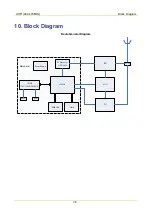
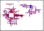
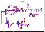
OMAP+FLASH
DMR OMAP PD500 U1
Model Name:
Prepare:
File No.:
Rev:
Date:
Page:
of
Part Name:
Hytera Communications Co.Ltd.
Check:
Approve:
A
3
12
Tuesday, October 22, 2013
OMAP+FLASH
DMR OMAP PD500 U1
Model Name:
Prepare:
File No.:
Rev:
Date:
Page:
of
Part Name:
Hytera Communications Co.Ltd.
Check:
Approve:
A
3
12
Tuesday, October 22, 2013
OMAP+FLASH
DMR OMAP PD500 U1
C1051
270pF
C1051
270pF
C1049
0.1uF
C1049
0.1uF
C1055
0.22uF
C1055
0.22uF
R1025 NC
R1025 NC
C1050
0.1uF
C1050
0.1uF
U1002A
OMAP5912ZZG-1
U1002A
OMAP5912ZZG-1
FLASH.A1
J8
FLASH.A2
D3
FLASH.A3
C1
FLASH.A4
E4
FLASH.A5
D2
FLASH.A6
F4
FLASH.A7
E3
FLASH.A8
J7
FLASH.A9
F3
FLASH.A10
G4
FLASH.A11
G3
FLASH.A12
G2
FLASH.A13
K8
FLASH.A14
H4
FLASH.A15
H3
FLASH.A16
K7
FLASH.A17
J2
FLASH.A18
J4
FLASH.A19
J3
FLASH.A20
F2
FLASH.A21
L8
FLASH.A22
K4
FLASH.A23
K3
FLASH.A24
L7
FLASH.A25
E1
FLASH.D0
N4
FLASH.D1
N2
FLASH.D2
N7
FLASH.D3
P2
FLASH.D4
P4
FLASH.D5
P7
FLASH.D6
R2
FLASH.D7
R3
FLASH.D8
R4
FLASH.D9
T2
FLASH.D10
T3
FLASH.D11
P8
FLASH.D12
U1
FLASH.D13
U3
FLASH.D14
T4
FLASH.D15
V3
FLASH.CLK/FLASH.CS2UOE
N3
FLASH.RDY/GPIO10
V2
FLASH.ADV
L4
FLASH.CS2/FLASH.BAA/FLASH.CS2L
M4
FLASH.BE1/FLASH.CS2UWE/GPIO60
M8
FLASH.BE0/FLASH.CS2UOE/GPIO59
L3
FLASH.CS0/GPIO62
M7
FLASH.CS1/FLASH.CS1L
M3
FLASH.CS3/GPIO3
N8
FLASH.OE
U4
FLASH.RP/FLASH.CS2UWE
W1
FLASH.WE
W2
FLASH.WP
V4
SDRAM.CS
G8
SDRAM.DQSH
C14
SDRAM.DQSL
D4
SDRAM.CAS
B4
SDRAM.DQML
C8
SDRAM.DQMU
D10
SDRAM.RAS
H7
SDRAM.WE
H8
SDRAM.A13
H11
SDRAM.A12
H9
SDRAM.A11
H10
SDRAM.A10
B8
SDRAM.A9
B12
SDRAM.A8
G9
SDRAM.A7
G11
SDRAM.A6
G12
SDRAM.A5
B9
SDRAM.A4
G10
SDRAM.A3
A1
SDRAM.A2
B6
SDRAM.A1
B2
SDRAM.A0
A2
SDRAM.BA1
C3
SDRAM.BA0
B3
SDRAM.D15
C12
SDRAM.D14
D12
SDRAM.D13
D13
SDRAM.D12
C11
SDRAM.D11
C13
SDRAM.D10
D11
SDRAM.D9
D14
SDRAM.D8
C10
SDRAM.D7
D8
SDRAM.D6
C4
SDRAM.D5
C7
SDRAM.D4
D5
SDRAM.D3
D7
SDRAM.D2
C5
SDRAM.D1
C6
SDRAM.D0
D6
SDRAM.CLK
C9
SDRAM.CLKX
D9
SDRAM.CKE
H12
R1013 10k
R1013 10k
C1081
0.22uF
C1081
0.22uF
C1052
270pF
C1052
270pF
C1054
0.01uF
C1054
0.01uF
R1016 NC
R1016 NC
C1053
1uF
C1053
1uF
U1001
W987D6HBGX6I
U1001
W987D6HBGX6I
DQ0
A8
DQ1
B9
DQ2
B8
DQ3
C9
DQ4
C8
DQ5
D9
DQ6
D8
DQ7
E9
DQ8
E1
DQ9
D2
DQ10
D1
DQ11
C2
DQ12
C1
DQ13
B2
DQ14
B1
DQ15
A2
A0
H7
A1
H8
A2
J8
A3
J7
A4
J3
A5
J2
A6
H3
A7
H2
A8
H1
A9
G3
A11
G2
A12
G1
A10
H9
CKE
F3
RAS
F8
UDQM
F1
BA1
G8
BA0
G7
WE
F9
CAS
F7
LDQM
E8
CS
G9
VSSA1
A1
VSSJ
1
J1
VSSE3
E3
VSSQ
A3
A3
VSSQ
C
3
C3
VSSQ
B7
B7
VSSQ
D
7
D7
V
DDE
7
E7
V
DDA
9
A9
V
DDJ9
J9
NC
E2
CLK
F2
V
DDQB
3
B3
V
DDQD3
D3
V
DDQA
7
A7
V
DDQC7
C7
L1005
BLM15PD121SN1
L1005
BLM15PD121SN1
1
2
C1056
1uF
C1056
1uF
R1034
100k
R1034
100k
R1017 0
R1017 0
U1003
S29GL128S10GHIV20
U1003
S29GL128S10GHIV20
A0
G1
A1
F1
A2
E1
A3
D1
A4
F2
A5
E2
A6
D2
A7
C2
A8
C6
A9
E6
A10
F6
A11
C7
A12
D7
A13
E7
A14
F7
A15
D8
A16
G8
A17
F3
A18
E3
A19
D6
A20
E5
A21
E8
A22
F8
A23
F5
DQ0
J2
DQ1
G3
DQ2
K3
DQ3
H4
DQ4
H5
DQ5
K6
DQ6
G6
DQ7
J7
DQ8
K2
DQ9
H3
DQ10
J3
DQ11
K4
DQ12
J6
DQ13
H6
DQ14
K7
DQ15
H7
CEf
H1
OE
H2
RESET
D4
WP/ACC
C4
VCCf
J4
CE1-ps
J1
RY/BYf
E4
NC1
A1
NC2
B1
NC3
C1
NC4
L1
NC5
M1
NC6
B2
NC7
L2
NC8
B3
UB
D3
LB
C3
WE
C5
CE2ps
D5
VCCps
J5
NC9
L3
NC10
B4
NC11
F4
NC12
G4
NC13
L4
NC14
B5
NC16
G5
NC17
K5
NC18
L5
NC19
B6
NC22
G7
NC23
L7
NC24
A8
VSS1
G2
VSS2
J8
NC25
B8
NC21
B7
NC20
L6
NC26
H8
NC27
L8
NC28
M8
4
4
OMAP-Memory电路
Summary of Contents for PD502
Page 1: ...PORTABLE...
Page 5: ...VHF 136 174 MHz...
Page 13: ...VHF 136 174 MHz Exploded View and Packaging Guide 7 3 2 Packaging Guide...
Page 18: ...VHF 136 174 MHz Circuit Description 12...
Page 43: ...PCB 3 9 PCB VHF 136 174 MHz...
Page 44: ...PCB 3 VHF 136 174 MHz...
Page 71: ...UHF1 400 470 MHz...
Page 79: ...UHF1 400 470MHz Exploded View and Packaging Guide 7 3 2 Packaging Guide...
Page 84: ...UHF1 400 470MHz Circuit Description 12...
Page 108: ...UHF1 400 470MHz PCB 36 9 PCB...
Page 109: ...UHF1 400 470MHz PCB 37...
Page 136: ...1616300000260 2014 03 17 L07157 4...