


Rev. 1.50
30
����st ��� �01�
Rev. 1.50
31
����st ��� �01�
HT66F0175/HT66F0185
A/D Flash MCU with EEPROM
HT66F0175/HT66F0185
A/D Flash MCU with EEPROM
*
*
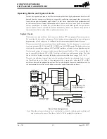
W r i t e r _ V D D
I C P D A
I C P C K
W r i t e r _ V S S
T o o t h e r C i r c u i t
P A 2
V S S
V D D
W r i t e r C o n n e c t o r
S i g n a l s
M C U P r o g r a m m i n g
P i n s
P A 0
Note: * may be resistor or capacitor. The resistance of * must be greater than 1kΩ or the capacitance
of * must be less than 1nF.
On-Chip Debug Support – OCDS
There is an EV chip named HT66V01x5 which is used to emulate the real MCU device named
HT66F01x5. The EV chip device also provides the “On-Chip Debug” function to debug the real
MCU device during development process. The EV chip and real MCU devices, HT66V01x5 and
HT66F01x5, are almost functional compatible except the “On-Chip Debug” function. Users can
use the EV chip device to emulate the real MCU device behaviors by connecting the OCDSDA
and OCDSCK pins to the Holtek HT-IDE development tools. The OCDSDA pin is the OCDS
Data/Address input/output pin while the OCDSCK pin is the OCDS clock input pin. When users
use the EV chip device for debugging, the corresponding pin functions shared with the OCDSDA
and OCDSCK pins in the real MCU device will have no effect in the EV chip. However, the two
OCDS pins which are pin-shared with the ICP programming pins are still used as the Flash Memory
programming pins for ICP. For more detailed OCDS information, refer to the corresponding
document named “Holtek e-Link for 8-bit MCU OCDS User’s Guide”.
Holtek e-Link Pins
EV Chip OCDS Pins
Pin Description
OCDSD�
OCDSD�
On-Chip Deb�� S�pport Data/�ddress inp�t/o�tp�t
OCDSCK
OCDSCK
On-Chip Deb�� S�pport Clock inp�t
VDD
VDD
Power S�pply
VSS
VSS
Gro�nd


