background image

3 - 10

Details of Servicing and Troubleshooting > Troubleshooting

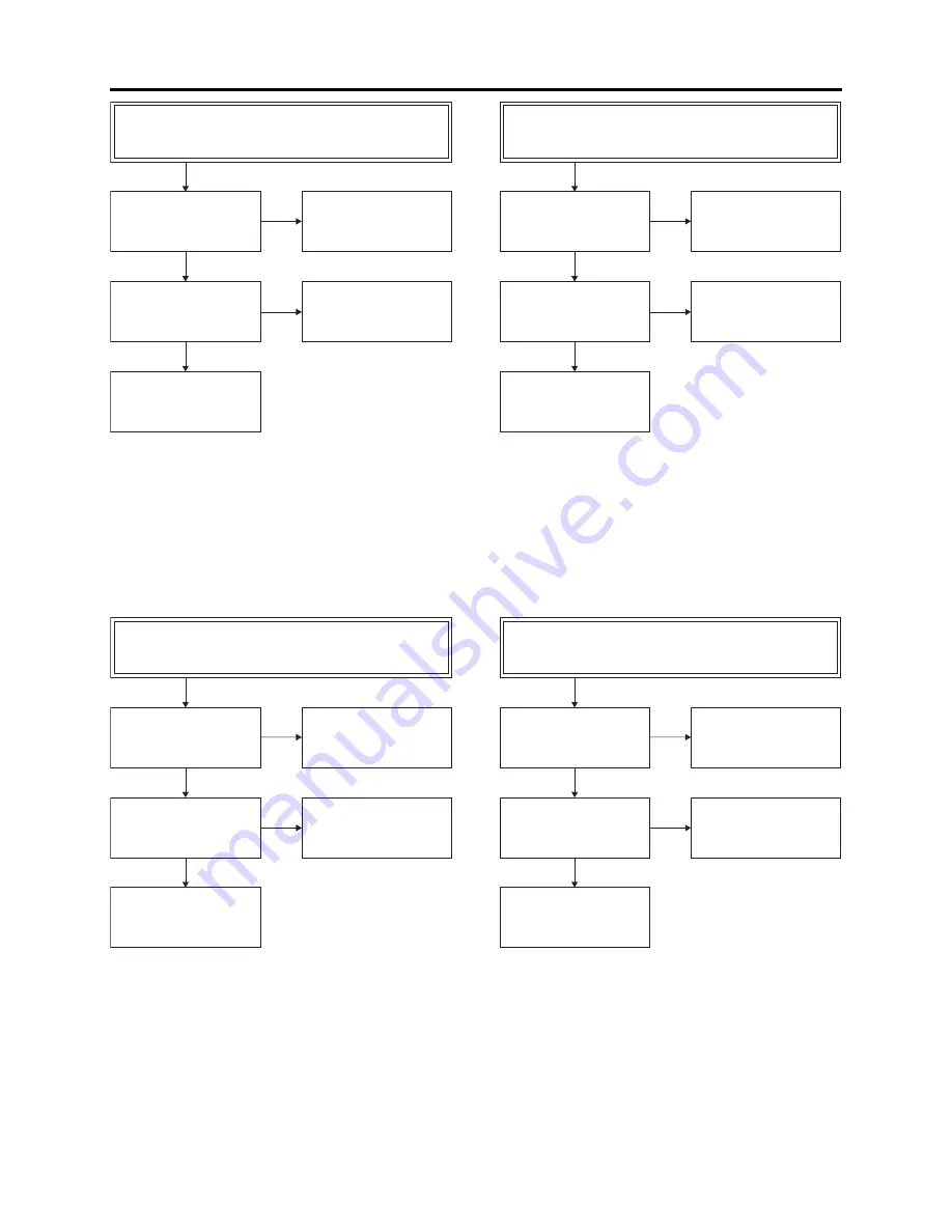
IC153 Pin1 :

Approx. 5.3V?

IC153 Pin4 :

Approx. 4V - 5V?

Check 5.3VA

on SMPS P.C.B.

Check the PWR_CTL_H

signal from IC701 Pin43.

NO

NO

YES

No 5.0VD

Check IC153, and

replace if necessary.

YES

IC151 Pin1 :

Approx. 3V - 3.8V?

IC151 Pin4 :

Approx. 4V - 5V?

Check D154 and D127

on SMPS P.C.B, and

replace if necessary.

Check the PWR_CTL_H

signal from IC701 Pin43.

NO

NO

YES

No 2.5V

Check IC151, and

replace if necessary.

YES

IC152 Pin1 :

Approx. 3.8V?

IC152 Pin4 :

Approx. 4V - 5V?

Check D127, and

replace if necessary.

Check the PWR_CTL_H

signal from IC701 Pin43.

NO

NO

YES

No 3.3V

Check IC152, and

replace if necessary.

YES

Is Vcc (5.3V)

supplied to Q158 Emitter?

R179 and R156 :

Approx. 0V?

Check 5.3VA

on SMPS P.C.B.

Check the STANBY_H

signal from IC701 Pin47.

NO

NO

YES

No SW_5.3V

Check Q158, and

replace if necessary.

YES

Summary of Contents for DV-DS163E

Page 1: ...SERVICE MANUAL SPECIFICATIONS AND PARTS ARE SUBJECT TO CHANGE FOR IMPROVEMENT HDD DVD RECORDER May 2006 SM0607 DV DS163E DV DS163E UK DV DS253E DV DS253E UK DO NOT RESELL OR DIVERT IMPROPERLY ...

Page 2: ...eous updating procedure 3 6 3 5 Troubleshooting 3 7 3 5 1 Troubleshooting electronic system 3 7 4 Disassembly and Reassembly 4 1 4 1 Order of Disassembly 4 1 4 2 Disassembly 4 2 1 Top Cover Fan 4 2 2 Front Block 4 3 3 TIMER 1 P C B TIMER 2 P C B Front Panel 4 3 4 MAIN P C B 4 4 5 Power Cable SMPS P C B 4 5 6 HDMI Block HDMI P C B 4 6 7 Front Frame DVD Block DVD Drive Unit LOADER P C B 4 7 8 HDD Bl...

Page 3: ... B Block Diagrams B 1 B 1 Overall Block Diagram B 1 B 2 SMPS Circuit Block Diagram B 2 B 3 POWER I O Board Circuit Block Diagram B 3 B 4 AUDIO VIDEO Circuit Block Diagram B 4 B 5 SYSTEM Circuit Block Diagram B 5 ...

Page 4: ...dentified by marking with a on the schematics and the parts list in this Service Manual The use of a substitute replacement component which does not have the same safety characteristics as the HITACHI recommended replacement one shown in the parts list in this Service Manual may create shock fire or other hazards Product safety is continuously under review and new instructions are issued from time t...

Page 5: ...observe the following cautions 1 Do not subject optical pickups to any severe vibrations or impact during movement installation or disassembly 2 When performing repair work do not perform disassembly any further than that described in this manual 3 Never turn the semi variable resistors for adjustment in optical pickup or DVD drive 4 NEVER look into the objective lens in optical pickup or directly...

Page 6: ...bject to any impact while the disk is rotating i e the head hitting against the disk breakage could result 2 Move the HDD approximately 2 minutes approximately 30 seconds for surveillance system devices after turning it off and unplugging its power cord from AC outlet The disk will still be rotating by inertia immediately after the HDD is turned off Subjecting the HDD to movement at this time coul...

Page 7: ...composition of alloy Sn is tin Ag is silver Cu is copper Bi is bismuth Pb is lead 3 Soldering iron for servicing The temperature of soldering iron tip must be adjusted according to the points to be soldered Use an antistatic soldering iron with thermal control function When removing components take care not to damage any surrounding component or pattern When attaching components observe the heatin...

Page 8: ...ist When you read them note the following regular indications 2 Values in schematic diagrams The values dielectric strength power capacitance and tolerances of the resistors excluding variable resistors and capacitors are indicated in the schematic diagrams using abbreviations Certain symbols are indicated for value units When you read them note the regular indications in tables below Safety Preca...

Page 9: ...cision components Refer to the following table and perform the designated appropriate servicing Any changes that occur in the service method will be published using service bulletin etc Do not perform any servicing other than that described in this manual 2 Fig 2 1 1 Component Location Component Service method a HDD Unit replacement b TIMER 2 P C B Component replacement c CARD P C B Component repl...

Page 10: ...d to Video mode Playable on regular DVD players after finalization Limited editing features DVD RW These Discs can be recorded on repeatedly Recordings can be erased then you can record again on the same Disc Playable on DVD RW compatible players automatically finalization The edited contents are playable on DVD RW compatible players only after finalization Recordings can be edited the title chapt...

Page 11: ...C s O NOT USE IRREGULARLY SHAPED S E G HEART SHAPED OR OCTAGONAL OING SO MAY RESULT IN MALFUNCTIONS s EPENDING ON THE RECORDING SOFTWARE THE FINALIZATION SOME RECORDED DISCS 2 27 OR 6 2 27 MAY NOT BE PLAYABLE s 6 2 27 6 2 27 AND 2 27 DISCS RECORDED USING A PERSONAL COMPUTER OR A 6 OR 2ECORDER MAY NOT PLAY IF THE DISC IS DAMAGED OR DIRTY OR IF THERE IS DIRT OR CONDENSATION ON THE 2ECORDER S LENS s ...

Page 12: ...DD 160GB Approx 48 hours XP mode 84 hours SP mode 156 hours LP mode 222 hours EP mode Video recording format Sampling frequency 27MHz Compression format MPEG 2 VBR support Audio recording format Sampling frequency 48kHz Compression format Dolby Digital Playback Frequency response DVD PCM 48 kHz 8 Hz to 20 kHz CD 8 Hz to 20 kHz DVD PCM 96 kHz 8 Hz to 44 kHz Signal to noise ratio More than 100 dB AU...

Page 13: ...163E 160GB DV DS161E ł Remote control DV DS253E DS163E DV RM253E DV DS253E UK DS163E UK DV RM253E UK DV DS251E DS161E DV RM251E DV DS161E UK DV RM251E UK Memory card slot For CF MD ST1 MD x1 For SD Mini SD MMC MMC Plus RS MMC MMC Mobile xD x1 For CF MD x1 For SD MMC SMC xD x1 DV input terminal x1 IEEE 1394 standard ł S Video input terminal x1 ł Video Audio input terminals x4 RCA x2 SCART x2 ł Comp...

Page 14: ...pter Markers Provided ł Changing Title Thumbnails Provided ł Making a New Playlist Provided ł Adding Title Chapters Provided ł Deleting Title Chapter Provided ł Deleting a Part Provided ł Time Search Provided ł Sort Provided ł Combining Titles Provided ł Divide Provided ł Combining Chapters Provided ł Moving a Playlist Chapter Provided ł Hide a Chapter Title Provided ł Playback Displaying Disc Inf...

Page 15: ...e REC The recorder is recording HDD The recorder is HDD mode DVD The recorder is DVD mode HDD DVD The recorder is dubbing TV Indicates when the recorder is in TV tuner mode Indicates when the recorder is in timer recording or a timer recording is programmed Indicates clock total playing time elapsed time title number chapter track number channel etc Remote Sensor Point the recorder remote control ...

Page 16: ...R RECORDING TEMPORARILY PRESS AGAIN TO EXIT PAUSE MODE 0 9 3TARTS PLAYBACK 0 7 2 3WITCHES THE RECORDER OR 2 0LAYS TRACKS IN RANDOM ORDER 2 3TARTS RECORDING 0RESS REPEATEDLY TO SET THE RECORDING TIME 2 3ELECTS THE RECORDING MODE 80 30 0 OR 0 2 0 4 2EPEAT CHAPTER TRACK TITLE ALL 2 3 54 3ETS THE OUTPUT RESOLUTION FOR 2 452 s 2EMOVES THE MENU s ISPLAY THE MENU OF A VIDEO WITH 0 3 3EARCH BACKWARD OR FO...

Page 17: ... 2IGHT ONNECT THE AUDIO OUTPUT OF AN EXTERNAL SOURCE UDIO SYSTEM 46 ONITOR 6 2 AMCORDER 6 5 54 EFT 2IGHT ONNECT TO A 46 WITH AUDIO INPUTS 8 IGITAL AUDIO OUT JACK ONNECT TO DIGITAL COAXIAL AUDIO EQUIPMENT 04 IGITAL AUDIO OUT JACK ONNECT TO DIGITAL OPTICAL AUDIO EQUIPMENT OOLING FAN 0OWER ORD 0LUG INTO THE POWER SOURCE 2 54 0ASSES THE SIGNAL FROM THE 2 TO YOUR 46 MONITOR 52 6 5 6 ONNECT TO A 46 WITH...

Page 18: ...THE OLBY IGITAL AND 0 OPTIONS TO 0 ON THE SETUP MENU s F YOUR 46 IS NOT EQUIPPED WITH 43 DECODER SET THE 43 OPTIONS TO ON THE SETUP MENU 4O ENJOY 43 MULTI CHANNEL SURROUND YOU MUST CONNECT THIS RECORDER TO A 43 COMPATIBLE RECEIVER VIA ONE OF THIS RECORDER S DIGITAL AUDIO OUTPUTS s 4HE ARROW ON THE CABLE CONNECTOR BODY SHOULD FACE UP FOR CORRECT ALIGNMENT WITH THE CONNECTOR ON THE RECORDER s F THER...

Page 19: ...hannel full range sound and one channel for sub woofer sound playback DRC Dynamic Range Control Adjusting the audio range of maximum and minimum levels dynamic range will improve audio signal when for example dialog is hard to hear or user is watching movies late at night DTS Digital Theater System Sound system as for movie theaters developed by US Digital Theater Systems Inc The number of channel...

Page 20: ...images will not quite fit on 4 3 screens There are two ways of displaying 16 9 images on 4 3 TV Pan Scan Cuts out the left and right ends of images and displays them on whole screen Letterbox Reproduces 16 9 images on 4 3 screens with black bands across the top and bottom of screen Playback Control PBC One format to play Video CD User can select desired screens and data while watching the displayed...

Page 21: ... the arrow 3 The disc lid d will open and the disc tray e will come out a few millimeters 4 Hold the both left and right ends of disc tray and pull out the tray in the direction of the arrow a Front Lid b Pin an extended clip etc c Eject Hole d Disc Lid e Disk Tray Details of Servicing and Troubleshooting 3 Fig 3 1 1 Removing Disc b e e c d d a 1 3 4 4 2 ...

Page 22: ...ight button 3 Use the cursor up and down buttons to choose Factory Set and press the ENTER button 4 Follow the instructions on screen hereafter to return the various settings to the factory defaults 3 2 2 HDD Format Execute HDD Format to delete all recorded data on HDD Be sure to execute this item after replacing a HDD so that the new HDD will be usable 1 Press the SETUP button on remote control 2...

Page 23: ...and check the operation sound of HDD unit HDD is faulty Replace it and recheck Is any operation sound heard in cases other than above No HDD is normal Yes Does playback stop at the same recorded point HDD is probably faulty Replace the HDD and recheck No Yes Recorder stops at the same point during HDD playback Ask customer whether the recorded contents can be erased and acquire approval HDD is nor...

Page 24: ... display 3 4 2 Method of starting up firmware update program 1 Turn the HDD DVD recorder on and press the OPEN CLOSE button 2 Insert the firmware disc 3 Press HOME button on the remote control to display the Home Menu screen Fig 3 4 3 4 Select the MOVIE Options appear 5 Select the DISC and press the ENTER button The screen for verifying update will appear Fig 3 4 4 6 Select the YES and press the ENT...

Page 25: ...g 3 4 5 will appear 2 Press the REC button on this HDD DVD recorder three times Both the current version of main firmware and the version of main firmware on the disc will appear on the screen Fig 3 4 6 3 Pressing the REC button on this HDD DVD recorder will start writing Fig 3 4 7 To cancel writing press the OPEN CLOSE button and remove the disc 4 When updating is complete the tray will open automa...

Page 26: ... To cancel writing press the OPEN CLOSE button 4 Turn the HDD DVD recorder off automatically 3 4 5 Main Loader firmware simultaneous updating procedure 1 To make firmware updating CD 1 Start a CD writer program and drag the main and loader firmware data files write them to the Root folder on CD 2 Change the volume name of CD to RH1000_UP 3 Write the main and loader firmware data to a CD R or CD RW in t...

Page 27: ...lied to IC101 Pin4 Replace F101 Replace BD101 Replace TH01 Check D102 and replace if necessary NO NO NO Replace D128 NO IC103 Pin1 Approx 2 5V Replace IC103 NO D121 Normal Replace D121 NO D122 Normal Replace D122 NO D124 Normal Replace D124 NO D125 Normal Replace D125 NO NO YES YES YES YES YES YES YES YES YES No 5 3VA D126 Normal Power Line on I O P C B Shorted Replace D126 NO YES D127 Normal Repl...

Page 28: ... Pin4 Approx 4V 5V Check D125 and replace if necessary Check the PWR_CTL_H signal from IC701 Pin43 NO NO YES YES No 5V for HDD DVD IC155 Pin1 Approx 13 5V IC155 Pin4 Approx 4V 5V Check D124 and replace if necessary Check the PWR_CTL_H signal from IC701 Pin43 Check C155 and replace if necessary NO NO YES YES No 12V for HDD DVD ...

Page 29: ...R_H signal from IC701 Pin44 NO YES 2 SMPS Circuit on I O P C B Is Vcc 14V supplied to Q164 Collector ZD151 Q164 Base Approx 12 5V Check D124 on SMPS P C B and replace if necessary Check Q164 and replace if necessary NO NO YES No 12V R171 Approx 5V Q156 Base Approx 0 7V Check the PWR_CTL_H signal from IC701 Pin43 Check Q156 and replace if necessary NO YES YES Is Vcc 33V supplied to Q162 Emitter Che...

Page 30: ...MPS P C B and replace if necessary Check the PWR_CTL_H signal from IC701 Pin43 NO NO YES No 2 5V Check IC151 and replace if necessary YES IC152 Pin1 Approx 3 8V IC152 Pin4 Approx 4V 5V Check D127 and replace if necessary Check the PWR_CTL_H signal from IC701 Pin43 NO NO YES No 3 3V Check IC152 and replace if necessary YES Is Vcc 5 3V supplied to Q158 Emitter R179 and R156 Approx 0V Check 5 3VA on ...

Page 31: ...prox 3V 3 3V Check 3 3V power supply Check Q159 and replace if necessary NO NO YES No 1 8V Check IC154 and replace if necessary YES Is Vcc FD supplied to Q163 Collector R184 and Q153 Collector Approx 12 5V Check D121 on SMPS P C B and replace if necessary Check Q163 and replace if necessary NO NO YES No SW_FD Check Q153 and replace if necessary YES Is Vcc 5 3V supplied to Q153 Emitter Q153 Base Ap...

Page 32: ... Vcc 3 3V supplied to PVM02 Pin19 21 YES NO Check 1 25V power supply Is Vcc 1 25V supplied to PVM02 Pin28 30 YES NO Check 2 5V power supply Is Vcc 2 5V supplied to PVM02 Pin6 YES NO Check 1 8V power supply Is Vcc 1 8V supplied to PVM02 Pin10 YES NO Check 5V power supply Is Vcc 5V supplied to PVM02 Pin23 P1D01 Pin1 Approx 12V P1D01 Pin4 Approx 5V Check SMPS Circuit Check SMPS Circuit NO NO YES Disc...

Page 33: ...essary YES NO Check SMPS Circuit YES Check Q801 Q802 Q803 Q805 Q806 Q807 Q808 and replace if necessary IC801 Pin 1 7 Is there a signal IC801 Pin8 12V NO YES NO Check SMPS Circuit YES IC803 Pin 21 22 25 26 Is there a signal NO IC803 Pin2 4 VCC 12V IC803 Pin32 33 SCL SDA NO Check SMPS Circuit YES Check IC803 and replace if necessary YES L806 L826 L825 L810 Is there a signal NO Check L806 L826 L825 L...

Page 34: ...heck MAIN P C B and replace if necessary OPTICAL COAXIAL R851 NO YES Check R851 and replace if necessary JK803 Pin2 5 2V NO YES Check R852 and 5 2V power supply Check JK803 and Optical cable C856 NO YES Check C856 and replace if necessary NO YES Check BD817 and replace if necessary Check JK802 and Coaxial cable BD817 ...

Page 35: ...s there a signal IC803 Pin2 4 VCC 12V IC803 Pin32 33 SCL SDA NO Check IC803 and replace if necessary YES Check IC707 and SW_12VG power supply NO IC901 Pin34 on I O P C B Or R999 RESET YES NO Check MAIN P C B and replace if necessary X901 24 576MHz clock oscillated YES NO Check X901 and replace if necessary R902 R913 R997 R962 R978 I2 C NO Check MAIN P C B and replace if necessary YES C901 Pin173 o...

Page 36: ...CC 12V IC803 Pin32 33 SCL SDA NO Check IC803 and replace if necessary YES Check IC707 and SW_12VG power supply NO IC901 Pin34 on I O P C B Or R999 RESET YES NO Check MAIN P C B and replace if necessary X901 24 576MHz clock oscillated YES NO Check X901 and replace if necessary R902 R913 R997 R962 R978 I2 C NO Check MAIN P C B and replace if necessary YES IC901 Pin173 on I O P C B and R903 Is there ...

Page 37: ...o COMPOSITE video signal Check JK802 and Cable connections PVM01 Pin14 18 22 Is there a signal NO YES Check MAIN P C B and replace if necessary IC802 Pin30 Is there a signal NO YES IC802 Pin1 16 5 3V NO YES Check SMPS Circuit Check IC802 and replace if necessary IC802 Pin29 Is there a signal NO YES IC802 Pin1 16 5 3V NO YES Check SMPS Circuit Check IC802 and replace if necessary AV1 AV2 AV3 IC803 ...

Page 38: ...YES C IC803 Pin21 22 25 26 Is there a signal YES NO IC803 Pin2 4 VCC 12V IC803 Pin32 33 SCL SDA Check IC803 and replace if necessary YES Check IC707 and SW_12VG power supply NO C926 Is there a signal AV1 AV2 C869 EU1_V_IN C871 EU2_V_IN Is there a signal NO Check TU701 Pin19 and replace if necessary Check JK801 L827 L818 Cable connections Input signal YES B YES B Check C842 L926 R946 and replace if...

Page 39: ... Check X901 and replace if necessary R962 R978 I2 C NO Check MAIN P C B and replace if necessary YES IC901 Pin108 on I O P C B and R930 VIN_CLK Is there a signal NO YES IC901 Pin3 31on I O P C B 1 8V IC901 Pin4 9 on I O P C B 3 3V Replace I O P C B YES Check 1 8V and 3 3V power supply NO C See When playing disc no RGB COMPONENT video signal and When playing disc no COMPOSITE video signal ...

Page 40: ...replace if necessary NO Check 3 3V power supply Is Vcc 3 3V supplied to PVM02 Pin19 21 YES NO Check 1 25V power supply Is Vcc 1 25V supplied to PVM02 Pin28 30 YES NO Check 2 5V power supply Is Vcc 2 5V supplied to PVM02 Pin6 YES NO Check 1 8V power supply Is Vcc 1 8V supplied to PVM02 Pin10 YES NO Check 5V power supply Is Vcc 5V supplied to PVM02 Pin23 DV mode switching Change to DV mode Using Rem...

Page 41: ... from the top of flowchart If multiple routes exist to the target component from the top of flowchart remove all the components on all the routes 4 Fig 4 1 1 Disassembly Flowchart Parts to remove Item Parts to remove Item Parts to remove Item Parts to remove Item Top Cover 4 2 1 4 2 1 Fan 4 2 4 MAIN P C B 4 2 5 Power Cable SMPS P C B 4 2 6 HDMI Block 4 2 6 HDMI P C B 4 2 7 Front Frame 4 2 7 DVD Bloc...

Page 42: ... Remove the top cover in the direction of the arrow 3 While extending both sides of the rear of top cover in the directions of arrows remove the top cover Fan b 4 Disconnect the connector of fan motor from SMPS P C B 5 Remove the two screws J a Top Cover b Fan c Fan Cover Fig 4 2 1 Top Cover Fan A M3X8 Black J M2 6X21 Black 3 a c b 4 1 A 1 A 1 A 1 A 5 J 3 2 Disassembly and Reassembly Disassembly ...

Page 43: ... 4 2 2 Front Block 3 TIMER 1 P C B TIMER 2 P C B Front Panel 1 Remove the three screws B 2 Disconnect the two connectors Information During reassembly attach the earth plates d to the specified positions making sure the orientation is correct a TIMER 1 P C B b TIMER 2 P C B c Front Panel d Earth Plate Fig 4 2 3 TIMER 1 P C B TIMER 2 P C B Front Panel 3 2 2 2 1 2 a b 1 B 1 B 1 B b d d d c a 2 2 B M3...

Page 44: ... O P C B b in the direction of the arrow The MAIN and I O P C B are directly joined via the connector Removing the MAIN P C B in a direction other than that of the arrow could damage the connector Caution during disassembly and reassembly Securely connect the MAIN and I O P C B a MAIN P C B b I O P C B c HDMI Block d SMPS P C B C M3X6 Gold 2 D 1 3 1 2 C 2 C 2 D d a b c D M2 6X24 Silver ...

Page 45: ...PS P C B from the I O P C B c in the direction of the arrow The SMPS and I O P C B are directly joined via the connector Removing the SMPS P C B in a direction other than that of the arrow could damage the connector Caution during disassembly and reassembly Securely connect the SMPS and I O P C B a Power Cable b SMPS P C B c I O P C B d HDMI Block e Rear Panel f MAIN P C B 4 C 4 C 4 C b a d f 5 1 ...

Page 46: ...t the unit of the HDMI block a 4 Remove the two screws H and remove the HDMI P C B b Caution during disassembly and reassembly Securely connect the HDMI P C B and the HDMI frame c a HDMI Block b HDMI P C B c HDMI Frame d MAIN P C B e SMPS P C B Fig 4 2 6 HDMI Block HDMI P C B 2 G 3 C 4 H 4 H e d 1 a c b C M3X6 Gold G M3X6 Black H M3X6 Silver ...

Page 47: ...ect the connector 5 Remove the four screws E 6 Remove the DVD block in the direction of the arrow DVD Drive Unit c LOADER P C B d 7 Disconnect the FFC from the LOADER P C B 8 Remove the LOADER P C B from the DVD drive unit in the direction of the arrow Caution during disassembly and reassembly Securely connect the LOADER P C B and the DVD drive unit a Front Frame b DVD Block c DVD Drive Unit d LOA...

Page 48: ...FFC from the HDD P C B 6 Remove the screw C 7 Remove the HDD P C B from the HDD in the direction of the arrow Caution during disassembly and reassembly Securely connect the HDD P C B and the HDD 8 Remove the six screws F and the HDD from HDD frame d a HDD Block b HDD P C B c HDD d HDD Frame e HDD Plate Fig 4 2 8A HDD Block Disassembly and Reassembly Disassembly 3 C 3 C a 4 2 1 C M3X6 Gold F M3 4X5...

Page 49: ...ve the three screws C 3 Remove the CARD P C B a in the direction of the arrow a CARD P C B Fig 4 2 9 CARD P C B Disassembly and Reassembly Disassembly 2 C 3 1 a C M3X6 Gold Unlock Pull out 8 F 8 F 8 F 8 F 6 C d c b 7 5 e Fig 4 2 8B HDD P C B HDD ...

Page 50: ...C B Disassembly and Reassembly Disassembly Fig 4 2 10 I O P C B 2 C 2 C 2 C a 1 K 1 K 4 C M3X6 Gold K M3X8 Black 11 Rear Panel 1 Remove the two screws K 2 Move the bottom section of rear panel in the direction of the arrow 3 Remove the rear panel in the direction of the arrow a Rear Panel K M3X8 Black 1 K 2 3 a Fig 4 2 11 Rear Panel ...

Page 51: ...omponent replacement A46 MAIN P C B Circuit board assembly replacement SMPS P C B Component replacement I O P C B Component replacement HDMI P C B Component replacement CARD P C B Component replacement 104 HDD Unit Unit replacement A60 DVD Drive Unit Unit replacement 463 463 463 463 463 463 463 463 463 468 468 468 468 452 280 250 CABLE2 463 463 463 CABLE5 463 410 410 410 410 410 468 468 468 468 46...

Page 52: ...THE UPDATED PARTS LIST FOR THIS MODEL IS AVAILABLE ON ESTA 5 2 ...

Page 53: ...2F 3F 4F 5F 6F 7F 8F 1F HDD PMV02 PMV01 40pin 40pin FAN MOTOR SMPS P1701 2pin 4pin PMV04 P1D01 16 pin 30 pin DVD DRIVE UNIT 40pin P104 LOADER 12V 5V 12V 5V FD FD 28VA 14VA 33VA 3 8VA 5 3VA PWR_CTL_H PML07 PML08 PMC09 PMH10 PMT05 PHM01 PVM01 PVM02 PVM03 PWVS1 VIDEO SELECT SW EURO AV2 EURO AV1 AV3 COMP COAXIAL OPTICAL AERIAL HDD UNIT PTM01 I O MAIN HDMI TIMER 2 TIMER 1 DV S AV4 CARD S 1 S Schematic ...

Page 54: ...B C D E F A B C D E F 8 7 6 5 4 3 2 1 8 7 6 5 NOTES NOTE NOTE NOTE BC121 T W 0 2 R148 T W 0 1uF 3 2 1 To POWER I O PWVS1 1E To FAN MOTOR To DVD HDD FH02 FH01 1000P 400VAC 1000P 400VAC 0 1u 275VAC 0 1u 275VAC EU01W UZ12BSC UZ 33BSD 33u 25V The following shows the neme of circuit and plug to which signal is connected and the address To MAIN 3A PG1001 1 2 To MAIN PG2001 3A VIDEO AUDIO R AUDIO L Name ...

Page 55: ... 1 8 7 6 5 To SMPS P1701 8E To TUNER SYSTEM 8F To TUNER SYSTEM 8E The following shows the neme of circuit and plug to which signal is connected and the address To MAIN 3A PG1001 1 2 To MAIN PG2001 3A VIDEO AUDIO R AUDIO L Name of citcuit diagram Address Name of citcuit diagram and plug Address 18K 18K 18K 10V KIA78R05API KIA78R33PI KIA278R25PI S 3 S 3 POWER Schematic Diagram I O P C B P m ...

Page 56: ...y To JACK 8D 8C To JACK 5D To DECODER 1E To JACK 5C To POWER 8D To JACK 8D To POWER 8A The following shows the neme of circuit and plug to which signal is connected and the address To MAIN 3A PG1001 1 2 To MAIN PG2001 3A VIDEO AUDIO R AUDIO L Name of citcuit diagram Address Name of citcuit diagram and plug Address P P MM1510XNRE X S524A60X51 SCT0 MN101D10F C735 470uF 6 3V S 4 TUNER SYSTEM M Schema...

Page 57: ...DECODER 7D To TUNER SYSTEM 8D To DECODER 8E To DECODER 1D The following shows the neme of circuit and plug to which signal is connected and the address To MAIN 3A PG1001 1 2 To MAIN PG2001 3A VIDEO AUDIO R AUDIO L Name of citcuit diagram Address Name of citcuit diagram and plug Address Z02W6 8V Z02W6 8V Z02W6 8V Z02W6 8V Z02W6 8V Z02W6 8V Z02W6 8V Z02W6 8V Z02W6 8V Z02W6 8V Z02W6 8V Z02W6 8V Z02W6...

Page 58: ...TEM 8E To JACK 5B 5C To JACK 5B To JACK 8C To JACK 8B To JACK 5C To JACK 5B SW_A_OUT_R SW_A_OUT_L The following shows the neme of circuit and plug to which signal is connected and the address To MAIN 3A PG1001 1 2 To MAIN PG2001 3A VIDEO AUDIO R AUDIO L Name of citcuit diagram Address Name of citcuit diagram and plug Address 120 120 120 120 120 120 120 120 SAA7137DHS S 6 DECODER Schematic Diagram ...

Page 59: ...7E 8E 1E 2F 3F 4F 5F 6F 7F 8F 1F 4 3 2 1 A B C D E F A B C D E F 8 7 6 5 4 3 2 1 8 7 6 5 TIMER 1 TIMER 2 SW901 POWER SW903 HDD DVD SW909 RESOLUTION SW907 CH SW906 REC SW904 STOP SW905 PLAY PAUSE SW908 CH SW902 OPEN CLOSE To MAIN PMT05 FV 834ND S 7 S 7 TIMER 1 TIMER 2 Schematic Diagram TIMER 1 TIMER 2 P C B R r R ...

Page 60: ...A 2B 3B 4B 5B 6B 7B 8B 1B 2C 3C 4C 5C 6C 7C 8C 1C 2D 3D 4D 5D 6D 7D 8D 1D 2E 3E 4E 5E 6E 7E 8E 1E 2F 3F 4F 5F 6F 7F 8F 1F 4 3 2 1 A B C D E F A B C D E F 8 7 6 5 4 3 2 1 8 7 6 5 S 8 S 8 HDMI Schematic Diagram ti To Be Report ...

Page 61: ...9 2 6 10 3 7 11 4 8 PVM01 Pin1 AOUT_IEC958 PVM01 Pin10 VOUT_G Y PVM01 Pin2 VOUT_R Pr PVM01 Pin18 VOUT_CVBS PVM01 Pin6 VOUT_B Pb PVM01 Pin22 VOUT_C PVM01 Pin9 VIN_CLK PVM02 Pin1 SDA PVM02 Pin3 SCL IC901 Pin108 27MHz X901 14 31818MHz ...

Page 62: ...55 12 5 75 5 75 5 75 13 0 01 0 01 0 01 14 5 70 5 70 5 70 15 0 01 0 01 0 01 16 5 70 5 70 5 70 17 0 00 0 00 0 00 18 0 00 0 00 0 00 19 0 00 0 00 0 00 20 5 70 5 70 5 70 21 5 81 5 81 5 81 22 5 81 5 80 5 80 23 5 74 5 74 5 73 24 5 70 5 70 5 70 27 5 73 5 73 5 73 28 3 31 3 26 3 33 29 2 47 2 62 2 35 30 2 47 2 62 2 35 31 1 88 1 88 1 80 32 5 05 5 05 5 05 33 5 07 5 07 5 07 34 0 00 0 00 0 00 IC808 CS4351 1 1 61...

Page 63: ...D D D D D D D D D 5 6D 6D D D D 7D D D D D D D D D D D D D D 7D 7 7 7 7D D D D D 7 7D 8D 1D 2E 3E 3E 3E E 3 4 4 4E 4 4 4 4E 4 5E 5E 5E 5E 6E 6E 6E 6 6E 7E E E 7E 7E E 7 7E E 7E E E E E E 7E E 7 7 8E 1E 2F 3F 4F 5F 6F 7F 8F 1F 4 3 2 1 A B C D E F A B C D E F 8 7 6 5 4 3 2 1 8 7 6 5 SIDE A C 1 C Circuit Board Diagrams a C 1 I O Circuit Board Diagram ar ...

Page 64: ...C 6C 6C 6 6 6C 6C C 6 7C 7 7C C C C C C C 7 7 7 7 8C 1C 2D 3 3 3 3D D D 3 D D D D 4D D D D D 4 4 4 5D D 5 5 5 5D 5 5D D D D 7D D 7D 7 7 7 7D D 7D 7D 7 8D 1D 2E 3E E E 3 3 3 3E 3 4E E 4E E 4E 4E E 4 6E E 6 6 6E 6E 6E 6E 6E 6 6E E 7E 7 7 7E 7 7E E E 7E 7 7E E 7E 7 8E 1E 2F 3F 4F 5F 6F 7F 8F 1F 4 3 2 1 A B C D E F A B C D E F 8 7 6 5 4 3 2 1 8 7 6 5 SIDE B C 2 I O Circuit Board Diagram D ...

Page 65: ... 3D D 4D D D 5D D 6D 7D 8D 1D 2 2E 3E 3E 4E 5E 6E 7E 8E 1E 2F 3F 4F 5F 6F 7F 8F 1F 4 3 2 1 A B C D E F A B C D E F 8 7 6 5 4 3 2 1 8 7 6 5 SIDE A SIDE B SIDE A SIDE B C 3 C 2 SMPS Circuit Board Diagram C 3 TIMER 1 Circuit Board Diagram C 4 TIMER 2 Circuit Board Diagram T a o 3 B C 2 SMPS Board Diagram o C 3 TIMER 1 Circuit Board Diagram r C 4 TIMER 2 Circuit Board Diagram i ...

Page 66: ...1D 2E 3E 4E 5E 6E 7E 8E 1E 2F 3F 4F 5F 6F 7F 8F 1F 4 3 2 1 A B C D E F A B C D E F 8 7 6 5 4 3 2 1 8 7 6 5 SIDE A SIDE A SIDE B SIDE B C 4 C 5 HDMI Circuit Board Diagram C 6 HDD Circuit Board Diagram 6 B DMI Board Diagram DMI Board Diagram C 5 HD C 5 HD D D am am Circuit Board Diagr Circuit Board Diagr C 6 HDD C 6 HDD C C ra ra ...

Page 67: ...RIVE SIO_SPI_CS0 SIO_SPI_CLK SIO_SPI_MISO SIO_SPI_MOSI MAIN HA 6 21 Flash 64M Bit IC1201 FLASH VIDEO 3 IN HA 1 5 23 22 PHY SAIN ASTEL PHY Buffer 74LVC541 IC1503 BUFFER SOCKET x2 SOCKET x2 HDD DRIVE ATAPI2_DATA 0 15 ATAPI2 _ VOUT_Y C VOUT_Y Pb Pr_R G B EURO AV2 Tuner TUNER SW AUDIO 3 IN AUDIO 4 IN AV_DEC Decoder SAA7137 IC901 AV DECODER IC803 U COM IC701 SYSTEM µP Latch 74LVT16373 IC1301 LATCH IC11...

Page 68: ...R SMOOTHING BLOCK D124 C123 L123 C133 3 8V RECTIFIER SMOOTHING BLOCK D127 C124 L124 C134 33V RECTIFIER SMOOTHING BLOCK D126 C126 R147 5 3V RECTIFIER SMOOTHING BLOCK D128 C125 L125 C135 T101 RECTIFIER SMOOTHING BLOCK D121 FR121 C120 R181 R191 R131 ZD121 RECTIFIER SMOOTHING BLOCK D122 C122 R122 5V RECTIFIER SMOOTHING BLOCK D125 C121 FEEDBACK BLOCK R141 R142 R143 R144 R145 R146 C143 PHOTO COUPLER IC1...

Page 69: ...T SW_12VG IC803 2 4 AV SW 33VT TU701 17 TUNER 3 3V IC703 3 6 AMP IC901 on I O P C B AV DECODER 1 8V Q702 D701 IC808 17 AUDIO DAC IC701 51 SYSTEM µP IC808 10 20 AUDIO DAC IC901 on I O P C B AV DECODER IC706 1 RESET IC701 37 SYSTEM µP SYS_5 3VA TU701 4 TUNER SW801 1 VIDEO SW 4 3 2 1 A B C D E F A B C D E F 8 7 6 5 4 3 2 1 8 7 6 5 B 3 B 3 POWER I O Board Circuit Block Diagram ...

Page 70: ...SW_FD FD FD 29VA 12V 5 3VA 5 2V 33VT 5VT 1 8V 3 3V 2 5V IC801 14VA 5 3VA FD I O TU_V_OUT DAC_A L R_OUT TPA TPA TPB TPB DV IN BIO_PHY_D 7 0 BIO_PHY_CLK BIO_LPS BIO_LREQ BIO_PHY_CTL0 BIO_PHY_CTL1 BIO_LINK_ON RST_PHY 1394_PD AUDIO Mute Block AUDIO MUTE BLOCK A_MUTE_ MUTE_L R L A_OUT_L R IC_OUT_L R IC904 IC903 TU_L R_OUT SECAM_AM A_SEL 5 0VD 1 25V TU_SECAM_H TU_SE_VL_H AFT RGB_SEL SCART 1 EURO AV1 AOU...

Page 71: ...1 DIS901 VFD FLD_CLK ENA_L FLD_TXD G 0 16 SIO_SPI_CLK SIO_SPI_MOSI SIO_SPI_CS 0 SIO_SPI_MISO IC1101 MPEG ENC DEC IC706 PWR_FAIL_L PWR_CTL_H SMPS POWER BOARD AV SW IC803 VPS IC707 DAV TIMER_H CV IN2 AFT IC704 RESET SMPS Block ON I O BOARD STANBY_H IC903 904 AUDIO SW IC_OUT_L IC_OUT_R SECAM_AM 4 3 2 1 A B C D E F A B C D E F 8 7 6 5 4 3 2 1 8 7 6 5 B 5 B 5 SYSTEM Circuit Block Diagram ...

Page 72: ...47 Milano Italia ITALY Tel 39 02 487861 Tel 39 02 38073415 Servizio Clienti Fax 39 02 48786381 2 Email customerservice italy hitachi eu com HITACHI Europe AB Box 77 S 164 94 Kista SWEDEN Tel 46 0 8 562 711 00 Fax 46 0 8 562 711 13 Email csgswe hitachi eu com HITACHI EUROPE S A S Lyon Office B P 45 69671 BRON CEDEX FRANCE Tel 33 04 72 14 29 70 Fax 33 04 72 14 29 99 Email france consommateur hitachi...

Reviews: