background image

10

PLC1/AVC5-UB

ACKNOWLEDGMENTS
AND TRADEMARKS

This LCD Television complies with VESA DDC2B specifications, Plug & Play is
a system with computer, peripherals (including monitors) and operating
system. It works when the monitor is connected to a DDC ready computer that
is running an operating system software that is capable for the plug & play.

When a Plug and Play PC is powered on, it sends a command to the Monitor
requesting identification. The Monitor sends back a string of data including its
characteristics.

TRADEMARK ACKNOWLEDGMENT

DDC   is a trademark of Video Electronics Standard Association.
IBM PC/AT and VGA are registered trademarkds of International Business Machines Corporation of the U.S.A.
Apple and Macintosh are registered trademarks of Apple Computer, Inc.
VESA is a trademark of a nonprofit organization, Video Electronics Standard Association.

This Class B digital apparatus meets all requirements of the Canadian Interference-Causing Equipment Regulations.

This Class B digital apparatus complies with Canadian ICES-003.

Cet appareil numérique de la classe B est conforme à la norme NMB-003 du Canada.

Cable Compatible Television Apparatus- Tèlèvision câblocompatible, Canada.

Notes on Closed Caption:

This LCD Television receiver will display television closed captioning, (

or 

), in accordance with

paragraph 15.119 of the FCC rules.

TM

TruBass and the SRS      

®

symbol are trademarks of SRS Labs, Inc.  TruBass technology is incorporated under license

from SRS Labs, Inc.

TABLE OF CONTENTS


Summary of Contents for 32HDL51M

Page 1: ...N These servicing instructions are for use by qualified service personnel only To reduce the risk of electric shock do not perform any servicing other than that contained in the operating instructions unless you are qualified to do so Before servicing this chassis it is important that the service technician read the IMPORTANT SAFETY INSTRUCTIONS in this service manual SAFETY NOTICE USE ISOLATION T...

Page 2: ...h is physical ground Using an insulation tester DC500V connect one of its leads to the AC plug jumper and touch with the other lead each exposed metal part antennas screwheads metal overlays control shafts etc particularly any exposed metal part having a return path to the chassis should have a resistor reading over 4MΩ Any resistance value below this range indicates an abnormality which requires ...

Page 3: ...the replacing work of the Panel module in order to protect not only the display area of the panel module but also the serviceman 6 Signal power supply P W B s and LCD driving circuits P W B s are assembled on the rear side of the LCD module take special care with this fragile circuitry particularly Flexible Printed Circuits bonded to surrounding edges of the panel They are not strong enough to wit...

Page 4: ...ent Electrostatically Sensitive ES Devices Some semiconductor solid state devices can be damaged easily by static electricity Such components commonly are called Electrostatically Sensitive ES Devices Examples of typical ES devices are integrated circuits and some field effect transistors and semiconductor chip components The following techniques should be used to help reduce the incidence of comp...

Page 5: ...ment IC in the circuit board 2 Carefully bend each IC lead against the circuit foil pad and solder it 3 Clean the soldered areas with a small wire bristle brush It is not necessary to reapply acrylic coating to areas Small signal Discrete Transistor Removal Replacement 1 Remove the defective transistor by clipping its leads as close as possible to the component body 2 Bend into a U shape the end o...

Page 6: ...his technique only on IC connections 1 Carefully remove the damaged copper pattern with a sharp knife Remove only as much copper as absolutely necessary 2 Carefully scratch away the solder resist and acrylic coating if used from the end of the remaining copper pattern 3 Bend a small U in one end of a small gauge jumper wire and carefully crimp it around the IC pin Solder the IC connection 4 Route ...

Page 7: ...against the soldering pads with tweezers or with a miniature alligator clip and apply heat to the pad area with a 30 watt iron until solder flows Do not apply heat for more than 3 seconds How to Replace Flat lC Required Tools Soldering iron iron wire or small awl De solder braids Magnifier 1 Remove the solder from all of the pins of a Flat lC by using a de solder braid 2 Put the iron wire under th...

Page 8: ...ad Please remove previous solder as much as possible from the soldering point When soldering please perfectly melt the lead free solder to mix well with the previous solder 3 Soldering iron for lead free solder Melting point of lead free solder is higher than solder containing lead Use of a soldering tool with temperature control and with much thermal capacitance is reccomended Reccomended tempera...

Page 9: ... an outlet on a circuit different from that to which the receiver is connected Consult the dealer or an experienced radio television technician for help Modifications The FCC requires the user to be notified that any changes or modifications made to this device that are not expressly approved by Hitachi Home Electronics America Inc may void the user s warranty Cables Connections to this device mus...

Page 10: ...f International Business Machines Corporation of the U S A Apple and Macintosh are registered trademarks of Apple Computer Inc VESA is a trademark of a nonprofit organization Video Electronics Standard Association This Class B digital apparatus meets all requirements of the Canadian Interference Causing Equipment Regulations This Class B digital apparatus complies with Canadian ICES 003 Cet appare...

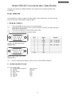
Page 11: ...refore the cable interface to the monitor should be male 1 3 The cable is configured in a null modem wiring scheme 1 4 A pin reference illustrations is provided below Figure 1 a Male 9 pin D sub Outside View Figure 1 b Female 9 pin D Sub Outside View 1 5 Electric Electrical specification is based on the current RS232C standard 2 Communication Format 2 1 Port Configuration 1 Communications System A...

Page 12: ... 10 11 12 13 14 Start Stop Figure 3 3 Television Answer Format Showing current Status The television responds with a 6 byte answer strings as follows Start 1 byte 02 Hex STX Response 4 byte Upper Data Lower Data Stop 1 Byte 03 Hex ETX 1 2 3 4 5 6 Start Stop Figure 4 4 Television Answer Format Status of Command Execution Acknowledgement 06 Hex ACK No Acknowledgement 15 Hex NAK ACK NAK Figure 5 Func...

Page 13: ...f 6 The television will always respond when an attempt to turn terminal mode on or off is made with either an ACK or a NAK 7 In the following cases even if the check box of menu is checked Terminal mode cannot be turned on Adjust mode While Event Timer and Timer Recording While Auto CH scan operates While Magic Focus operates While upgrade operates 8 Write function in terminal mode will write data...

Page 14: ...sent to the television as shown in table 3 2 1 2 The television will respond with an answer as shown in table 3 2 2 In the event that a command is rejected by the television an Hex 15 will be sent to the PC Table 3 2 2 Answer format from television to PC 1 Character Code Example 0 9 R 30 39 A F R 41 46 Start Stop Received byte 1 2 3 4 5 6 7 8 9 10 11 12 13 14 Contents Start 1st 2nd 3rd 4th 5th 6th...

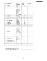
Page 15: ... Range of Commands Table 3 3 4 Setting Item List Setting Command 1st R W 3rd 4th No Function Hex Control Hex OSD E2PROM Command Format 1 1 POWER 6E R W 0000 Info Write c 2 INPUT 6F R W 0000 Info Write c 3 Volume 27 R W 0000 Volume Bar c 4 Balance 28 R W 0000 No OSD c 5 Treble 2B R W 0000 No OSD c 6 Bass 2A R W 0000 No OSD c 7 Audio Mute 29 R W 0000 No OSD c 8 Picture Mode A4 R W 0003 Day Night c 9...

Page 16: ...10 Brightness 0 60 Step 30 11 Color 0 60 Step 30 12 Tint 0 60 Step 30 13 Sharpness 0 60 Step 30 14 Color Temperature 0 High 1 Medium 2 Standard 3 Black White 15 Aspect 0 16 9 Std 1 16 9 Zoom 2 4 3 Std 3 4 3 Expand 4 4 3 Zoom 5 4 3 Zoom 2 16 Info 0 Off 1 On 0 17 Direct CH 0 9 Key Code 0 9 0 9 18 Direct Channel 0 19 Direct Channel Select 0 20 Virtual HD 0 1080I 1 540p 0 21 Auto Movie Mode 0 Off 1 On...

Page 17: ...en the unit is Terminal Mode On If the Terminal Mode is activated when the Auto Link Setting is in Stand By The Auto Link operation will be cancelled The Urgent Broadcast Signal will take precedence when Terminal Mode is on with the CableCARD installed The Magic Timer function is disabled when Terminal Mode is On 2 Other Terminal Control Considerations Terminal Mode will remain On when you turn th...

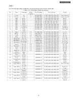
Page 18: ...ete command 4 3 Figure 6 shows the 14 byte string formatted in Hex Characters for the ìPower On Functionî 1 2 3 4 5 6 7 8 9 10 11 12 13 14 Start Stop 02 6 E 0 0 0 0 0 0 0 0 0 1 Figure 6 4 4 Figure 7 shows the ìPower Onî function converted to Hex Code set 1 2 3 4 5 6 7 8 9 10 11 12 13 14 Start Stop 02 36 45 30 30 30 30 30 30 30 30 30 31 Hex Character Hex Code 0 30 1 31 2 32 3 33 4 34 5 35 6 36 7 37...

Page 19: ...0000000001 323930303030303030303031 Set to On 17 Picture Mode Set to Day 0 A40000000000 413430303030303030303030 Set to Day 18 Picture Mode Set to Night 0 A40000000001 413430303030303030303031 Set to Night 19 Contrast Set to 59 60 590000000059 353930303030303030303539 Set to 59 20 Brightness Set to 29 30 1F0000000029 314630303030303030303239 Set to 29 21 Color Set to 29 30 100000000029 31303030303...

Page 20: ...43030303030303030303030 Key code to 0 37 Direct CH CH D00000010000 443030303030303130303030 CH 38 Direct CH Select Select CH D00000020000 443030303030303230303030 CH Select 39 Virtual HD Select 1080i 0 D30000000000 443330303030303030303030 Select 1080i 40 Virtual HD Select 540p 0 D30000000001 443330303030303030303031 Select 540p 41 Auto Movie Mode Auto Movie Off D40000000000 4434303030303030303030...

Page 21: ... of the complete TV set and conditions the signal before it arrives to the monitors The 32 monitors contain the displaying device which is the LCD display panel module and the driving circuitry which receives the signal from the AVC center and after processing delivers the image to the display module This HITACHI Service Manual is intended for the qualified service personnel and it contains the ne...

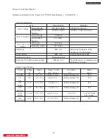
Page 22: ...ain 1080i Sub ANT A B Video 480i 1080i With Main RGB Sub All video signal except PC DM 6Mode 4 3 Standard 16 9 Standard 4 3 Expanded Zoom 1 Zoom 2 16 9 Zoom Full Normal Real Real 42 VGA 55 VGA SVGA XGA WXGA With Auto Movie Mode On Off 4Mode High Medium Standard Black White RGB VIDEO1 2 3 4 5 ANT A B IEEE1394 Photo Input With Main ANT A B Video 480i Sub ANT A B Video 480i 1080i VGA UXGA 1H 24KHz 10...

Page 23: ...23 PLC1 AVC5 UB Specification Features 2 of 2 ...

Page 24: ...er voltage 1V 60Hz 2 Input Video Signal Color Bar Supplied by AVC 3 Input Audio Signal Standard Burst Audio Signal Supplied by AVC 4 Setting Set the power consumption to be the maximum by User Control As for Audio output set the waveform distortion to be 10 5 Temp Humidity Normal 6 Pre heat run Over 30min 7 Others Set for shipment ...

Page 25: ... its maximum of rated value Power Factor 90 min Except Stand by mode Incoming Current 50Apeak or less Guaranty for sudden power outage 20msec min No malfunction or damage even at 20msec or more Output Specification Output Voltage V Range V Rating Current Min Max A Fluctuation V Ripple mVp p 5V STB 5V 4 8 5 2 0 4A 0 02 0 54 Setting Voltage 4 200 5V Vcc 5V 4 8 5 2 0 8A 0 3 0 Setting Voltage 4 200 12...

Page 26: ...OW OFF Audio Control Function 6 Matrix Surround ON OFF No Control Item Display Communication with AVC Contrast 1 Contrast 0 100 VIDEO Setting 1 Color Temperature Change over HIGH MED LOW B W 2 Input Terminal Mode RGB VIDEO Color Temp RGB Display R G HIGH B 00 FF R G MED B 00 FF R G LOW B 00 FF R G Color Temperature Adjustment Only while the AVC Service Mode is set B W B 00 FF Others 1 Peak Brightn...

Page 27: ...ncel Measuring Accumulated ON time To answer the accumulated time of ON mode by the request of AVC If the address of EEPROM doesn t have the designated data below ensure automatic initialization is executed and the data is written EEPROM Address Designated Data EEPROM Automatic Initialization Key Operation Sub Power SW To be able to change over ON Stand By mode SII169 Configuration DATA Setting Wh...

Page 28: ...Vp p Set up level 0V 3 Apply white raster signal into COMPONENT input terminal of AVC jig 4 Set user control to Day mode Picture mode 5 Confirm that the mode is set as Factory setting mode 6 Aspect Video EXPANDED PC FULL Preparation 2 1 Set service adjustment menu to DEVICE ADJUST MODE LCD 2 Set WBC to 0 Adjustment 1 Perform the following adjustment with the remote control 2 Set the CRT color anal...

Page 29: ...IUM 5 After receiving White raster signal step down the two or one among Adjustment of R G B DRIVE MEDIUM and adjust the value shown below 1 Perform the following adjustment with the remote control 1 Same as Video color temperature adjustment HIGH 2 Set the CRT color analyzer CA 100 at the center of the panel At least one of the data should be FF Remarks Specification Video Color temperature MED x...

Page 30: ...fication Video Color temperature STD x 0 314 0 005 y 0 327 0 005 4 Ensure that Adjustment of R G B DRIVE STD are all set as FF 3 Set color temperature to MEDIUM 5 After receiving White raster signal step down the two or one among Adjustment of R G B DRIVE STD and adjust the value shown below 1 Perform the following adjustment with the remote control 2 Set the CRT color analyzer CA 100 at the cente...

Page 31: ...ture adjustment HIGH Specification PC Color temperature B W x 0 335 0 005 y 0 343 0 005 3 Ensure that Adjustment of R G B DRIVE B W are all set as FF 4 After receiving White raster signal step down the two or one among Adjustment of R G B DRIVE B W and adjust the value shown below 1 Perform the following adjustment with the remote control 2 Set the CRT color analyzer CA 100 at the center of the pa...

Page 32: ...ld be FF Write Adjustment of x and y data value of video color temperature to the following Video Color Temperature PC Color Temperature R G B DRIVE MEDIUM Data R G B DRIVE MEDIUM Data R G B DRIVE STD Data R G B DRIVE STD Data R G B DRIVE B W Data R G B DRIVE B W Data Color temperature correction setting This setting should be done after color temperature adjustment 1 Set service adjustment menu t...

Page 33: ...ing TV VIDEO offset 2 2 White raster B W 5400K x 0 335 0 01 y 0 343 0 01 HIGH COOL 12000K x 0 268 0 01 y 0 283 0 01 MIDIUM NORM 9300K x 0 285 0 01 y 0 293 0 01 STD WARM 6500K x 0 314 0 01 y 0 327 0 01 2 Color Temp Setting when inputting RGB offset 2 2 6 25 White window B W 5400K x 0 335 0 01 y 0 343 0 01 when inputting TV VIDEO selecting Super 1 window 370 cd or more Color temp High when 100 ampli...

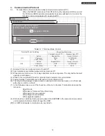
Page 34: ...ilure 1 No picture and No sound _Monitor AVC both LED Lighting Green Disconnect the Monitor connection cables Monitor_ Check burn in Mode 1 Trouble of Monitor Check the plug cable of Monitor AVC or Trouble of AVC OK Note 1 Burn in Mode There is burn in mode as method of displaying an image by the monitor part independent If it goes into burn in mode test signals such as white raster and monochrome...

Page 35: ... PLC1 AVC5 UB Yes _Monitor AVC both LED Lighting Red Disconnect the Monitor connection cables When power ON is carried out with AVC simple substance power LED is green Trouble of Monitor Trouble of AVC No ...

Page 36: ...hen it is made two screens are right and left the same Is OSD displayed correctly Yes Yes Yes No Trouble of AVC No Trouble of AVC No TV CH VIDEO INPUT and PC INPUT the same with an image 3 No sound or fault of sound noise etc Trouble of AVC IS audio monitor output terminal correctly Yes Yes No Trouble of AVC Check the plug cable of Monitor AVC or Trouble of Monitor ...

Page 37: ...37 PLC1 AVC5 UB No When carrying out operation of swivel is OSD of not available displayed Trouble of Monitor Yes Check the plug cable of Monitor STAND It is not failire 4 Swivel does not operate ...

Page 38: ...D 5 12V LCD 5 12V 3 8 GND GND 8 4 IR_OUT IR_OUT 4 1 D 1 8V D 1 8V 1 4 LCD 5 12V LCD 5 12V 4 9 GND GND 9 5 GND GND 5 2 D 1 8V D 1 8V 2 5 GND GND 5 10 GND GND 10 6 DM_PR DM_PR 6 3 GND GND 3 6 GND GND 6 11 PANEL DET PANEL DET 11 7 DM_PB DM_PB 7 4 GND GND 4 7 GND GND 7 12 ON OFF ON OFF 12 8 GND GND 8 5 DM 3 3V DM 3 3V 5 13 BRT BRT 13 9 DM_YH DM_YH 9 6 DM 3 3V DM 3 3V 6 14 GND GND 14 10 GND GND 10 7 DM...

Page 39: ...essing LCD Panel Unit Drain Driver Timing Converter LVDS Receiver Signal Controller DC DC Converter TMDS Receiver Audio Signal Gate Driver LED PWB Sensor Window Digital Audio Amplifier Filter unit Sub Woofer Output LVDS Transmitter AVC I F Signal Power Audio Power Connector 2 Systems LCD Panel Module 21 Power Unit Super TFT LCD Inverter FC Block Diagram Circuit Block Diagram ...

Page 40: ...STB5V 3 3V REG LCD Panel Module Filter PWB AC120V LED PWB RC Sensor Window LED Digital Audio Amplifier CPU TMDS Receiver LVDS Transmitter Signal Audio PWB Audio Processing 12 5V 10V 5V 12 5V Power Unit 24V 12V 12V AC INLET Swievel Inverter 24V BACK TO ADJUSTMENTS ...

Page 41: ...L_ON ARESETSCDT CPUDATA0 7 PBLK XRST EXTLD XCPUEN CPUCLK SWLDET CPDET SW_R SW_L FIN RIN TXD0 AVDET MUTE SPRLY SDA1 SCL1 FVPP MD1 RES RXD TXD RLED GLED REM L R LCD Microcomputer From AVC MPU Control Block Diagram Power Swivel Driver FC STB 5V SUBSW Power unit PROGRAM Writing 16MHz Power unit ...

Page 42: ...h Memory 62 Byte For storage of system software Mask ROM Version Included Built in RAM byte 2k byte For system work System Clock 16 Number of I O Port 66 SP OUT Lch SP OUT Rch MUTE CONT SCL1 SDA1 Lch IN Rch IN NJW1163 MASTER VOL BALANCE TONE CONT SURR ON OFF DYNAMIC BASS ON OFF M887M4690 PMT LIP SYNC TAS51220CA DIGITAL POWER AMP 12V PCM1802 A D SUB WOOFER OUT MUTE 3 3V TAS5001PFB DIGITAL POWER AMP...

Page 43: ...ymbol Pin No V DC 1 5v to 12v 1 5v 2 5v to 12v 2 _ 3 5v to 12v PSC2 3 GND PPL 4 5v to 12v 4 _ 5 GND 5 _ 6 GND 6 _ 7 GND Symbol Pin No V DC Symbol Pin No V DC 1 30v 1 5v 2 GND 2 3 3v 3 GND PSU 3 _ 4 5v 4 _ 5 5v 5 GND PPS 6 GND 7 GND 8 12v 9 12v 10 GND 11 GND 12 11v 13 11v ...

Page 44: ..._ 8 _ 9 _ 9 _ Symbol Pin No V DC Symbol Pin No V DC 1 5 0v 1 1 8v 2 _ 2 1 8v 3 _ 3 0v 4 _ 4 0v PJIC1 5 _ PFP2 5 3 3v 6 _ 6 3 3v 7 _ 7 3 3v 8 _ 8 0v 9 _ 9 0v Symbol Pin No V DC Symbol Pin No V DC 1 _ 1 24v 2 _ 2 24v 3 5v 3 24v 4 _ 4 24v 5 _ 5 24v JSW 6 _ PMS1 6 0v 7 _ 7 0v 8 _ 8 0v 9 _ 9 0v 10 _ 10 0v 11 _ 11 _ 12 _ 12 _ 13 _ 13 _ 14 0v ...

Page 45: ... PMH 10 0V 30 _ 50 0v 11 9 0v 31 _ 12 9 0v 32 0v 13 0v 33 _ 14 0v 34 0v 15 5 0v 35 _ 16 5 0v 36 0v 17 _ 37 _ 18 _ 38 0v 19 _ 39 _ 20 _ 40 0v Symbol Pin No V DC Pin No V DC 1 _ 21 3 3V 2 _ 22 3 6V 3 _ 23 3 6V 4 _ 5 _ 6 _ 7 0v Symbol Pin No V DC 8 _ 1 5 5v 9 _ 2 5 5v PMS1 10 _ 3 0v 11 0v PFP1 4 0v 12 5 4v 5 5v 13 0v 6 5v 14 _ 7 0v 15 5 6v 16 5 6v 17 0v 18 0v Symbol Pin No V DC 19 0v 1 _ 20 3 6v PAN ...

Page 46: ... value of the parts is subject to be altered for improvement Signal 1 of 5 PRODUCT SAFETY NOTE Components marked with a and shaded have special characteristics important to safety Before replacing any of these components read carefully the PRODUCT SAFETY NOTICE of this Service Manual Don t degrade the safety of the receiver through improper servicing BASIC CIRCUIT DIAGRAM PCLI AVC5 UB Signal 1 of ...

Page 47: ...lue of the parts is subject to be altered for improvement Signal 2 of 5 PRODUCT SAFETY NOTE Components marked with a and shaded have special characteristics important to safety Before replacing any of these components read carefully the PRODUCT SAFETY NOTICE of this Service Manual Don t degrade the safety of the receiver through improper servicing BASIC CIRCUIT DIAGRAM PCLI AVC5 UB Signal 2 of 5 4...

Page 48: ...lue of the parts is subject to be altered for improvement Signal 3 of 5 PRODUCT SAFETY NOTE Components marked with a and shaded have special characteristics important to safety Before replacing any of these components read carefully the PRODUCT SAFETY NOTICE of this Service Manual Don t degrade the safety of the receiver through improper servicing BASIC CIRCUIT DIAGRAM PCLI AVC5 UB Signal 3 of 5 4...

Page 49: ...iagram the value of the parts is subject to be altered for improvement Signal 4 of 5 PRODUCT SAFETY NOTE Components marked with a and shaded have special characteristics important to safety Before replacing any of these components read carefully the PRODUCT SAFETY NOTICE of this Service Manual Don t degrade the safety of the receiver through improper servicing BASIC CIRCUIT DIAGRAM PCLI AVC5 UB Si...

Page 50: ...lue of the parts is subject to be altered for improvement Signal 5 of 5 PRODUCT SAFETY NOTE Components marked with a and shaded have special characteristics important to safety Before replacing any of these components read carefully the PRODUCT SAFETY NOTICE of this Service Manual Don t degrade the safety of the receiver through improper servicing BASIC CIRCUIT DIAGRAM PCLI AVC5 UB Signal 5 of 5 5...

Page 51: ...lue of the parts is subject to be altered for improvement Filter 1 of 1 PRODUCT SAFETY NOTE Components marked with a and shaded have special characteristics important to safety Before replacing any of these components read carefully the PRODUCT SAFETY NOTICE of this Service Manual Don t degrade the safety of the receiver through improper servicing BASIC CIRCUIT DIAGRAM PCLI AVC5 UB Filter 1 of 1 5...

Page 52: ... UL CSA VDE SEMKO SEV DEMKO NEMKO BSI FIMKO 5 AC Inlet SUP C14608 F 8A 250V EP00013 E901 Markings With set 6 PWB MONITOR PWB MCL E 67 JA0575 B Markings 7 Power Code COD 125V10A UL CSA EV01841 E01 Markings UL CSA 8 LCD Display Panel Module FLT TX80D16VC0CA B DD0068 A Markings UL CSA 9 Power Unit POWP62783 HA0152 U1 Markings UL CSA List of Security Components Application MODEL 32HDL51M Item Name P C...

Page 53: ...53 PLC1 AVC5 UB ...

Page 54: ...54 PLC1 AVC5 UB ...

Page 55: ...55 PLC1 AVC5 UB ...

Page 56: ...00722 AV PWB ASSEMBLY HCY503 ASSEMBLY UE23413 JP07641 JP07651 HP00773 UNX2RF ANTENA SWITCH JP07641 A HDMI PWB JP07651 A 1 19 1 20 ME03381 POW PWB COVER AVC75 CHASSIS FRAME ASSENBLY NQ24621 FRONT BRACKET AVC75 NA71911 REAR METAL PLATE NA71921 FUNCTION BUTTOM PC06151 PWB FIX METAL NA71931 FUNCTION SW PWB JP07641 A 1 21 AVC76 EXPLODED VIEW PARTS LIST TOP CASE AVC75 4 6 4 4 4 3 6 11 5 6 7 2 6 6 6 9 16...

Page 57: ...57 PCL1 AVC5 UB EXPLODED VIEW MONITOR TABLE OF CONTENTS MODEL 32HDL51 ...

Page 58: ...Supply Unit Signal Audio PWB PSC2 PPS PSU PSL PPL PDS PSW PPU2 E901 One Turn 2 NOTE 2 Refer to 3rd page of Wire Dressing drawing for descritions and preparations of 2 3 4 5 and 6 6 3 ECN1 EPU1 EPU1 EPU1 ESU EPS ESL ESC2 EPL EPL ESD1 ESU ClamptheconnectorsE902and E903withthePigTailHolder N01 N01 N01 N01 N01 ESC2 E903 EPU1 E902 ESW ESC2 ECN1 EDS EPU1 ESU EPS ESW EPL ECN1 ESL EPS EPL ESC2 ESL PSC2L E...

Page 59: ... 2 2 2 2 Signal Audio PWB E901 2 2 2 2 2 ECN1 ESC2 EPU1 EAS2 E902 E903 E902 E903 ESU EPS EPL ESL ESD1 ESU EAS1 ESC2 920 N01 EDS Hold the Ferrite Core N01 in the top by a SK Binder 920 Cut the remainding end of SK Binder Please ensure no more than 3mm gap between Ferrite Core and EDS connector terminal N01 N01 N01 N01 N01 N01 N01 EAS2 EAS1 EAS1 EAS1 EAS2 Clamp and make one turn to the connectors EC...

Page 60: ... Plug Pin Posts as shown on the 1 This Drawing shows the wire dressing and connectors connection of PLC1 Specification ESW E902 E903 EAS1 EAS2 EPU1 EDS ESC2 EPS ESU ESL EPL ECN1 PPU1 PDS PSC2 PPS PSU PSL PPL P801 Inverter 2 Wires should be fixed into Lead Holder surely and locked if available 1 Wires should be fixed inside Lead Clamp and locked if available 6 When closing ferrite core the claw of ...

Page 61: ...rt Specification Connection of E902 E903 to E901 AC Inlet Metal Chassis Metal Chassis 6 Preparation of EDS foil tape P ZX02821 L 180mm Envolve the EDS connector by copper Cut and prepare ESD1 P EF24041 as follows 30mm 30mm Twist and sold the ESD1 preparation as follows Insulate the copper tape by twisting adhesive tape P 9436431 L 185mm To LCD Panel To Signal Audio To LCD Panel To Signal Audio To ...

Page 62: ...62 PLC1 AVC5 UB This page left blank intentionally ...

Page 63: ...PRINTED CIRCUIT BOARDS 63 PCL1 AVC5 UB ...

Page 64: ...PRINTED CIRCUIT BOARDS 64 PCL1 AVC5 UB X X Symbol Components Location Side B SIGNAL AUDIO BD Side B Location ...

Page 65: ...PRINTED CIRCUIT BOARDS 65 PCL1 AVC5 UB AC CONNECTION BD SP TERMINAL L SP TERMINAL R LED P W B FILTER P W B ...

Page 66: ...29R CEC100M16 EWMT105 C115 0893232R CAP 1608CHIP 100000PFZF25V TAPE C116 AD00629R CEC100M16 EWMT105 C151 0893232R CAP 1608CHIP 100000PFZF25V TAPE C152 0893232R CAP 1608CHIP 100000PFZF25V TAPE C153 0893208R CAP 1608CHIP 1000PFKB 50V TAPE C154 0893208R CAP 1608CHIP 1000PFKB 50V TAPE C170 0893204R CAP 1608CHIP 470PFKB 50V TAPE C171 AA01144R CERAMIC CAP 1608 B 1 0UF 16V C172 0893205R CAP 1608CHIP 560P...

Page 67: ...493 0893232R CAP 1608CHIP 100000PFZF25V TAPE C402 0893232R CAP 1608CHIP 100000PFZF25V TAPE C494 AD00631R CEC220M16 EWMT105 C405 AA00931R CAP CERAMIC 2012 1UF 10V C495 AA01141R CERAMIC CAPACITOR 0 1UF 16V C406 AA01111R CERAMIC CAPACITOR 1 0UF 6 3V C496 AA01141R CERAMIC CAPACITOR 0 1UF 16V C407 AA01111R CERAMIC CAPACITOR 1 0UF 6 3V C4A6 AA01141R CERAMIC CAPACITOR 0 1UF 16V C408 0893232R CAP 1608CHIP...

Page 68: ...CAPACITOR C5P2 AA01141R CERAMIC CAPACITOR 0 1UF 16V CP04 0893023R CAP 2125 CHIP 47000PF K B 25V C901 AN01443S ACROSS CAPA 0 1UF 250V RE104 CP05 0893031R CAP 2125CHIP 1000PFKB 50V TAPE C902 AN01443S ACROSS CAPA 0 1UF 250V RE104 CP09 0893027R CAP 2125 CHIP 100000PF K B 25V TAPE C903 AN01443S ACROSS CAPA 0 1UF 250V RE104 CP10 0893031R CAP 2125CHIP 1000PFKB 50V TAPE C904 AJ00195R CAP CERAMIC CK45 F2EA...

Page 69: ...100000PFZF25V TAPE CW52 AA00966R CERAMIC CAPACITOR 4 7UF 6 3V CV57 AA01101R CERAMIC CAPACITOR 1UF 10V F CW53 AA00966R CERAMIC CAPACITOR 4 7UF 6 3V CV58 0893135R CAP 1608CHIP 470PFJCH 50V TAPE CW54 AA00966R CERAMIC CAPACITOR 4 7UF 6 3V CV59 0893232R CAP 1608CHIP 100000PFZF25V TAPE CW55 AD00629R CEC100M16 EWMT105 CV60 0893213R CAP1608CHIP 2200PFKB 50V TAPE CW56 AD00629R CEC100M16 EWMT105 CV61 AD0062...

Page 70: ... CIRCUITS L512 BA00887R LBC2518 CHIP COIL 10UH L901 BZ05742 LINE FILTER 8 0MH I001 CK38994U MICRO COMPUTER M30626FHPFP B L902 BZ05741 LINE FILTER 5 6M I002 CK37052R ANALOG MONOLITHIC IC BD4742G L904 2123462M FERRITE BEADS CORE B 2 3UH I003 CK39652R DIGITAL MONOLITHIC IC BR24L32FJ WE2 L905 BZ01421R COIL FERRITE BEAD BL02RN1 R62T4 I004 CK50121R ICCD4053BPWR L907 2125806N FILT COIL LHL08 47UH I101 CK...

Page 71: ...LAG AC INLET SK 1019 Q932 1323293R TRS CHIP 2SC4617 TL R S JA01 2672041 MINI HEADPHONE JACK Q934 1323294R TRS CHIP 2SA1774 TL R S Q935 CA00983R TRS CHIP DTC144EE TL TRANCISTORS Q936 CA00983R TRS CHIP DTC144EE TL Q937 1323293R TRS CHIP 2SC4617 TL R S Q001 1323392 TRS CHIP UMX1N QA01 1323392 TRS CHIP UMX1N Q002 CA01301R TRS CHIPNDC7002N QA02 1323392 TRS CHIP UMX1N Q070 1323293R TRS CHIP 2SC4617 TL R...

Page 72: ...6K OHM R019 0790024R RES CHIP 1 16W 100 OHM R0E4 0790051R RES CHIP 1 16W 10K OHM R020 0790024R RES CHIP 1 16W 100 OHM R0F1 0790024R RES CHIP 1 16W 100 OHM R022 0790001R CHIPRESISTORRECJUMPER 1 16C16T1608 R0F2 0790024R RES CHIP 1 16W 100 OHM R023 0790059R RES CHIP 1 16W 47K OHM R0F3 0790001R CHIPRESISTORRECJUMPER 1 16C16T1608 R025 0790046R RES CHIP 1 16W 4 7K OHM R0F4 0790051R RES CHIP 1 16W 10K OH...

Page 73: ...IP 1 16W 15K OHM R323 0790024R RES CHIP 1 16W 100 OHM R208 0790001R CHIPRESISTORRECJUMPER 1 16C16T1608 R324 0790037R RES CHIP 1 16W 1 0K OHM R209 0790024R RES CHIP 1 16W 100 OHM R325 0790037R RES CHIP 1 16W 1 0K OHM R210 0790024R RES CHIP 1 16W 100 OHM R326 0790044R RES CHIP 1 16W 3 3K OHM R211 0790024R RES CHIP 1 16W 100 OHM R328 0790024R RES CHIP 1 16W 100 OHM R213 0790001R CHIPRESISTORRECJUMPER...

Page 74: ...5R RES CHIP 1 16W 680 OHM R465 0790037R RES CHIP 1 16W 1 0K OHM R4M7 0790001R CHIPRESISTORRECJUMPER 1 16C16T1608 R466 0790024R RES CHIP 1 16W 100 OHM R4M8 0790027R RES CHIP 1 16W 180 OHM R467 AQ00164R CHIP RESITOR 1 16W 75OHM TAPE R4M9 0790001R CHIPRESISTORRECJUMPER 1 16C16T1608 R468 0790041R RES CHIP 1 16W 1 8K OHM R4N0 0790024R RES CHIP 1 16W 100 OHM R469 0790041R RES CHIP 1 16W 1 8K OHM R4N1 07...

Page 75: ...0790044R RES CHIP 1 16W 3 3K OHM R910 0188157M RES CARBON FLM 100K J 1 2W R583 0790042R RES CHIP 1 16W 2 2K OHM R913 AT02525R METAL OXIDE RESISTOR 100OHM 3W R584 0790042R RES CHIP 1 16W 2 2K OHM R915 0790001R CHIPRESISTORRECJUMPER 1 16C16T1608 R585 0790042R RES CHIP 1 16W 2 2K OHM R916 0100069M RES CARBON FLM 1 8W 1 5K JB R586 0790024R RES CHIP 1 16W 100 OHM R931 0188091M RDL 1R0J1 02LT R587 07900...

Page 76: ... 16W 100 OHM RA36 0790037R RES CHIP 1 16W 1 0K OHM RV12 0790059R RES CHIP 1 16W 47K OHM RA37 0790061R RES CHIP 1 16W 56K OHM RV13 0790058R RES CHIP 1 16W 39K OHM RA38 0790051R RES CHIP 1 16W 10K OHM RV14 0790024R RES CHIP 1 16W 100 OHM RA39 0790061R RES CHIP 1 16W 56K OHM RV15 0790046R RES CHIP 1 16W 4 7K OHM RA41 0790001R CHIPRESISTORRECJUMPER 1 16C16T1608 RV16 AQ00191R RES CHIP 1 16W 750 OHM TAP...

Page 77: ...RES CHIP 1 16W 1 5K OHM RW69 AQ00215R RES CHIP 1 16W 6 2K OHM TAPE RV95 AQ00194R RES CHIP 1 16W 1 0K OHM TAPE RW70 AQ00182R RES CHIP 1 16W 360 OHM TAPE RV96 AQ00214R RES CHIP 1 16W 5 6K OHM RW71 0790051R RES CHIP 1 16W 10K OHM RV97 0790024R RES CHIP 1 16W 100 OHM RW72 AQ00215R RES CHIP 1 16W 6 2K OHM TAPE RV98 0790043R RES CHIP 1 16W 2 7K OHM RW73 AQ00182R RES CHIP 1 16W 360 OHM TAPE RV99 0790024R...

Page 78: ...5 B 16CT XV02 BP01241 OSCILLATOR 3 58 49U C466 AA01802R CCC103K50 B 16CTMCH18 XV03 BP01241 OSCILLATOR 3 58 49U C467 0800353R CAP ELECTRO 470UF M 16V XV04 2168771 VFL CSB503F30 C468 AA01814R CCC104K25 B 16CT XV05 2168771 VFL CSB503F30 C473 0800359R CAP ELECTRO 1000UF M 10V XV06 BE00431R 6MHZ LOW PASS LC FILTER C474 0800359R CAP ELECTRO 1000UF M 10V XV07 BE00431R 6MHZ LOW PASS LC FILTER C475 0800359...

Page 79: ...100K OHM INTEGRATED CIRCUITS R437 0790024R RES CHIP 1 16W 100 OHM R438 0790059R RES CHIP 1 16W 47K OHM IC401 CK39281R ANALOG MONOLITHIC IC NJW1136 R439 0790049R RES CHIP 1 16W 8 2K OHM IC402 CK35311R NJM2192AM R440 0790001R CHIPRESISTORRECJUMPER 1 16C16T1608 IC403 CK31991R ANALOG MONOLITHIC IC BU4052BCF E2 R441 0790001R CHIPRESISTORRECJUMPER 1 16C16T1608 IC404 CK39291R ANALOG MONOLITHIC IC TA2021 ...

Page 80: ...80 PLC1 AVC5 UB ...

Reviews: